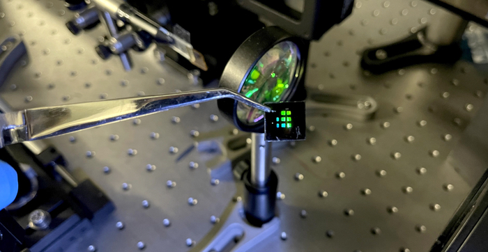
Quantum dot IR laser is CMOS compatible

IFCO team develop distributed feedback laser devices of PbS colloidal quantum dots on top of alumina substrate
In a recent paper published in Nature Photonics, Guy Whitworth, Mariona Dalmases, and Nima Taghipour from ICFO (The Institute of Photonic Sciences in Spain) led by Gerasimos Konstantatos have reported the achievement of a colloidal quantum-dot-based infrared laser source operating at room temperature, compatible with CMOS technology and tuneable to emit in the telecommunications window, an important milestone needed for classical or quantum communications.
Colloidal quantum dot (CQD) technology is based on a solution processed optoelectronic material platform that has demonstrated already its potential for infrared optoelectronics with high performance CMOS compatible photodetectors and light emitting diodes (LEDs). The realisation of an infrared CQD laser though had remained elusive.
Previous to this finding, the team had already been working on an experiment where they were able to demonstrate stimulated emission and optical gain of quantum dots on thin films, but what they were lacking was actually inserting this setup into a cavity to achieve lasing.
Infrared QD Lasing at room temperature
To find the ideal cavity for the experiment, the team of researchers took a distributed feedback cavity (DFB), spincoating atop a thin layer of PbS CQDs as the optical gain medium. By concomitantly tuning the size of the dots and the geometrical characteristics of the DFB to optimise the cavity resonance with the gain spectrum of the quantum dots they managed to demonstrate lasing emission across the eye-safe optical communication infrared spectrum and at room temperature, thus, possibly finding the last piece of the jigsaw puzzle for silicon photonics.
In addition, the researchers went a little further and engineered the surface of the dots in order to suppress electronic trap states in order to favor stimulated emission. They made use of a robust doping of the quantum dots to demonstrate lasing emission at lower pumping intensities, an achievement that opens a new path towards more practical implementations.
Gerasimos Konstantatos comments: “the results of this study are considered a major breakthrough in the field of CQD optoelectronics. This discovery may facilitate fully integrated silicon photonics, paving the way towards low-cost solution processed and CMOS integrated lasing sources for on-chip comm or LIDAR applications. Before, further advances are needed to optimise the material in order to demonstrate lasing under continuous wave or nanosecond excitation, which makes our next milestone.”
'Solution-processed PbS quantum dot infrared laser with room-temperature tunable emission in the optical telecommunications window' by G. L. Whitworth et al; Nature Photonics volume 15 (2021)


