
III-V Epi: a need for speed
Recently launched UK foundry services provider, III-V Epi, intends to accelerate epitaxial structure manufacture for lasers, HEMTs and more. Rebecca Pool talks to CTO, Richard Hogg, to find out how.
In July this year, III-V Epi launched to bring new III-V devices to market as quickly as possible. Led by UK industry veterans that hail from Gas Sensing Solutions, quantum tech hub, Quantic, and the University of Glasgow, the new company is already providing myriad wafer foundry services that rely on MBE and MOCVD to commercial firms and research organisations around the world.
III-V Epi's MBE and MOCVD epitaxial structures are being used in lasers, LEDs, photodetectors, HEMTs and more. And key customers to date include an Asia-based tech giant, UK start-up, Vector Photonics, laser equipment suppliers, defence organisations and several universities - with more of the same coming soon.

Richard Hogg from III-V Epi and the University of Glasgow.
“Myself and colleagues have worked together in the past and it was a natural progression to launch the company - we believe there's a massive unmet need here for low to medium volume [wafer production],” asserts Richard Hogg, III-V Epi chief technical officer, head of The Electronic and Nanoscale Engineering Division at Glasgow University, and chair of the scientific advisory board at Vector Photonics.
“In the past, all of III-V Epi's partners have had problems getting epi-wafers fabricated as [foundries] have been busy making, say, hundreds of thousands of VCSELs for handsets, mice or datacoms applications,” he says. “But as soon as you come away from an application that isn't in an iPhone or Samsung phone, your volumes are down and you may only need a dozen wafers - so we're focusing on low to medium volume and prototype III-V epitaxial structures for device applications.”
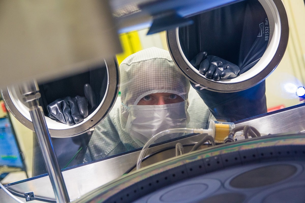
Right now, III-V Epi is using two MBE systems and two MOCVD reactors, with each instrument handling two to four inch wafer sizes. Recently developed structures include 980 nm VCSELs, antimonide photodetectors on GaAs substrates, novel multi-colour LEDs and Vector Photonics' photonic crystal surface emitting lasers (PCSELs). The company routinely performs regrowth in InP and GaAs-based systems while its InP distributed feedback (DFB) MOCVD re-growth processes have been qualified for 1310 nm DRB lasers.
On a different tack, Hall Effect measurements were recently carried out for a partner that had fabricated devices on a newly-commissioned reactor. And the company is also working with other UK-based Universities on developing routes to generating and commercializing intellectual property.
For now, the company is firmly sticking to antimonide, arsenide and phosphide materials, but alternative materials systems may follow in the future. “We're busy enough with three atoms right now,” laughs Hogg. “But there's always a possibility we could expand to nitrides or more exotic materials.”
From concept to structures
In a typical scenario, III-V Epi will spend some time working with customers to define an exact device design. This could, for example, involve converting a software simulation to a realistic design with specified layers and tolerances.
“We might ask, do you really want that tolerance on layer 17? And the customer might say no, but it is critical to layer 22,” explains Hogg. According to the CTO, this process can take time, but once the final design is decided, the company will typically fabricate the necessary structure in eight to ten weeks.
III-V Epi currently has two engineers running its MBE systems and four engineers running its MOCVD reactors across its three partner organisations, a set-up that Hogg reckons could be unique to the UK. “We've got this mixed usage situation where we have both MBE and MOCVD capabilities with neither within a university building,” he says. “Many of the engineers working with III-V Epi's partners are from Glasgow University, and it has just made sense to collaborate – we've got so much knowledge about manufacturing and we can bring this together with our research and development.”
In recent weeks, III-V Epi joined the European Photonics Industry Consortium (EPIC) and company growth is now expected. It's early days but Hogg and colleagues anticipate strong demand for the materials systems they can manufacture, and at some point expect to recruit highly skilled tools operators and tool setters to ramp volumes.
“Our fast turnaround times are critical at the moment,” says Hogg. “So much compound semiconductor capacity [is tied up] with a few big companies and getting spare capacity anywhere can be difficult.”
“We're going to want to have the ability to ramp up volumes by using operators to run our tools overnight so we can manufacture 24/7,” he adds.


