
Lateral gallium oxide MESFETs power ahead
Devices are first to combine high breakdown voltage with a high lateral figure-of-merit
Engineers in the US are claiming to have broken new ground for the all-round performance of lateral ß-Ga2O3 MESFETs. Their devices are said to be the first to combine a high breakdown voltage with a high lateral figure-of-merit, which is aided by realising a low specific on-resistance.
Spokesman for the team, Fikadu Alema from Agnitron, believes that these MESFETs are promising contenders for providing highly efficient power switching at high voltages. This strength could drive deployment of this device in power supplies, power transmission, electric grid integration and electric vehicles.
Alema and co-workers, including a team led by Sriram Krishnamoorthy, who has recently moved from the University of Utah to UCSB, argue that the strong performance of their ß-Ga2O3 MESFETs demonstrates that high-quality material can be produced with a conventional device process flow. Epilayers were grown by MOCVD at Agnitron Technology.
Devices based on ß-Ga2O3 can employ vertical and lateral geometries. The team has pursued the latter, partly because it leads to: fewer processing steps; simplifies packaging and integration requirements; and allows the fabrication of devices with different dimensions on the same wafer, enabling the formation of a range of transistors that target different operating voltages and frequencies. In addition, lateral devices aid thermal management, thanks to the channel being closer to the surface, which enhances heat extraction.
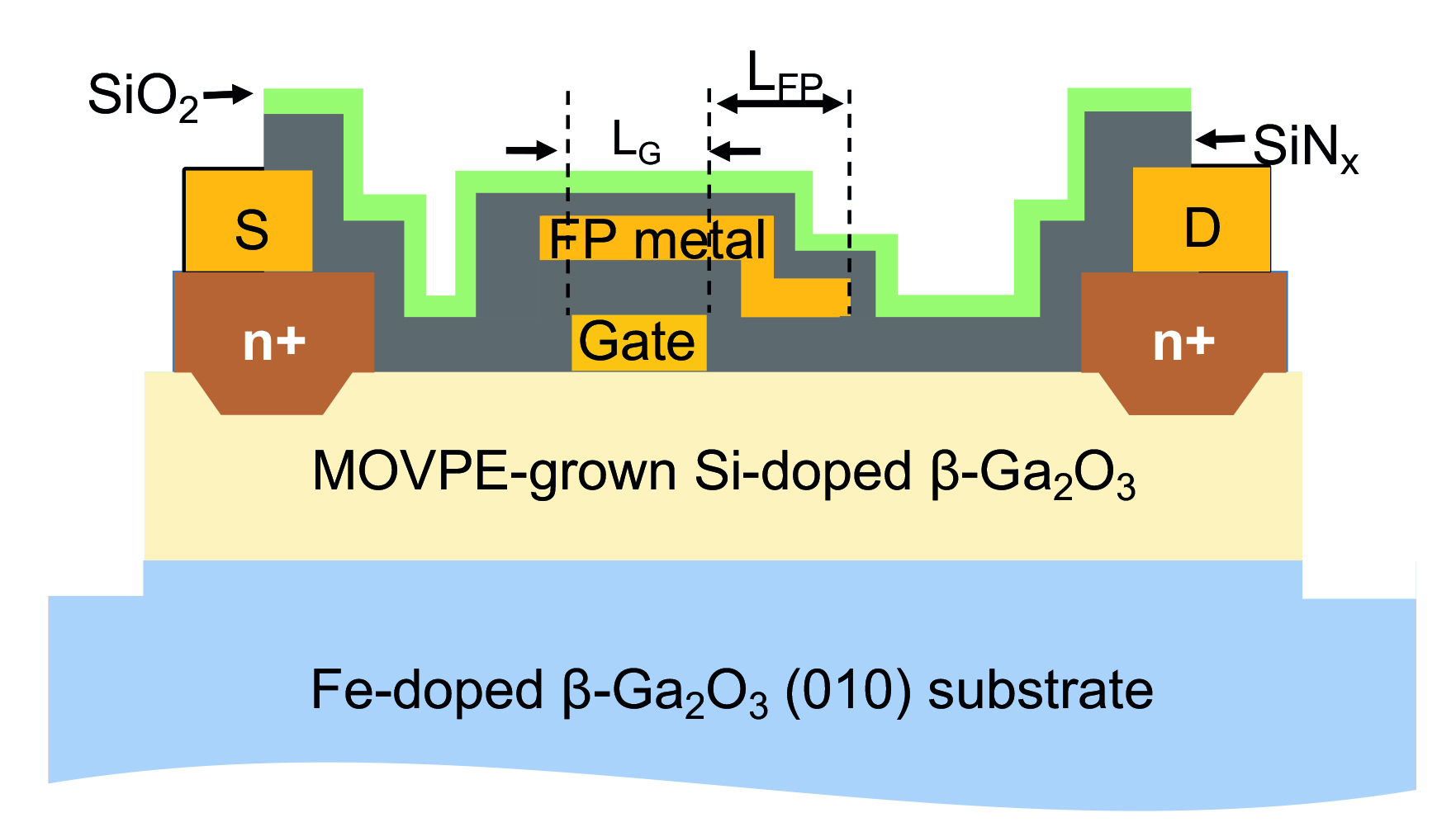
The team made their devices on 10 mm by 15 mm semi-insulating ß-Ga2O3 substrates that are iron-doped, formed by edge-defined film-fed growth, and produced by Novel Crystal Technology. On this substrate, cleaned by HF, the engineers deposited a 230 nm-thick layer of ß-Ga2O3doped with silicon at a density of around 3.6 x 1017 cm-3. According to Hall measurements, the charge in the channel and its mobility are 5.7 x 1012 cm-2 and 95 cm2 V-1 s-1, respectively.
To isolate the mesa and selectively grow source and drain ohmic contacts, the team turned to MOCVD regrowth, using a Ni/SiO2 mask pattern. Dry etching with an inductively coupled plasma provided a contact recess etch, with this step removing about 10-20 nm of the ß-Ga2O3 layer. For the regrown n+ layer, silicon doping is around 2.6 x 1020 cm-3. A combination of photolithographic pattering, lift-off, evaporation, and annealing formed ohmic source/drain contacts to the regrown layer. Electron-beam evaporation realised the Schottky gate.
Some MESFETs featured a gate-pad-connected field plate, formed by electrically connecting a gate field plate metal to the gate pad outside the device mesa. This architecture protects the channel region from dry-etching plasma damage, which occurs in the conventional gate field plate etch process flow.
The researchers have compared the performance of devices with and without a field plate. For MESFETs with a gate-to-source spacing of 1 µm, a gate length of 2.8 µm, and a gate-to-drain distance of 2.4 µm, on-resistance fell from 63.2 Ωmm to 55.8 Ωmm with the addition of the field plate. Transmission line measurements on structures produced with this approach to processing have a contact resistance of just 1.4 Ωmm, a figure ten times less than that associated with a previous generation of devices, thanks to the introduction of a low etch rate for dry etching of the contact recess.
Electrical measurement showed that adding a field plate cut on-resistance by 14 percent, increased on-current by 13 percent and boosted transconductance by 13 percent. For devices with 10 µm and 20 µm gate-to-drain lengths, breakdown voltages exceeded 2.4 kV and more than 3 kV. For the former device, the lateral figure of merit is 355 MΩ cm-2.
Alema says that the goals for the future include increasing the breakdown voltage to beyond 10 kV, and developing devices for delivering high output currents while accommodating blocking voltages of more than 1 kV.
REFERENCE
A. Bhattacharyya et al. IEEE Electron. 42 1272 Dev. Lett. (2021)


