
Shifting to 200 mm silicon carbide
Introducing larger wafers will accelerate the production of power electronic devices in fully depreciated 200 mm fabs
BY SANTHANARAGHAVAN PARTHASARATHY FROM GT ADVANCED TECHNOLOGIES
The goal of achieving carbon neutrality has gained momentum worldwide. Many steps are being taken to transform our global energy system, including a dramatic reduction in reliance on fossil fuels. The adoption of wide-bandgap semiconductors made from materials like SiC will provide energy-efficient devices that have almost no losses, creating a sustainable path to achieving net zero carbon emission.
Today’s power converters, including AC-DC rectifiers, AC-AC transformers, DC-DC converters and DC-AC inverters, tend to employ silicon-based power electronic devices – the IGBT, short for insulated gate bipolar transistor, is among the most commonly used. However, demands for faster switching frequencies, high power ratings, high conversion efficiencies and high-temperature operation are driving the adoption of devices made from SiC. This wide-bandgap semiconductor combines a bandgap that is three times that of silicon with a thermal conductivity that’s also three times higher and a breakdown field that is ten times greater, making devices made from SiC a perfect choice for these operations.
Shipments of SiC power devices, which are made on native single-crystal substrates, have climbed in recent years. This has enabled SiC to move out of the lab and establish itself as a mainstay for power electronic devices, especially when breakdown voltages greater than 900 V are required.
The foundation for commercialization of SiC power devices came in 1999, when 50 mm diameter wafers hit the market, selling for $495 a piece. While that seems an eye-watering price today, at the time this was considered a breakthrough. Now the majority of SiC power electronic devices, such as Schottky barrier diodes, MOSFETs, junction field-effect transistors and cascodes, are built on 150 mm wafers, with fabrication taking place in fully depreciated 150 mm and 200 mm fabs that have become available as wafer sizes in the silicon industry have transitioned to 300 mm.
To provide year-on-year productivity growth in the semiconductor industry, engineers tend to pull on five well-known levers: shrinking device dimensions, introducing a new device design, improving equipment productivity, increasing line yield, and migrating to a larger wafer size. Of these five, the latter offers considerable gains, which is why there is so much interest in the development of 200 mm SiC wafers.
The obvious benefit of increasing the surface area of the wafer is that it drives up the number of devices, or die, that it can yield. This increase diminishes fabrication cost per device, since the number of process steps remains the same (see Table 1).
Readily available fab capacity
Today silicon-based power devices, such as the IGBT, are mass-produced on 300 mm silicon wafers. That’s because Tier 1 integrated device manufacturers (IDMs) have invested billions of dollars over the last few years on 300 mm fabs for making silicon power electronics.
Thanks to the migration of silicon power device manufacturing to 300 mm fabs, fully depreciated 150 mm and 200 mm fabs are now available for SiC production. Supporting this venture, IDMs have added toolsets for SiC device fabrication. These include : MOCVD reactors capable of growth up to 1600 °C; high-energy, high-temperature implanters; dopant-activation furnaces; metrology equipment; wafer-level testing; and die singulation tools. These fabs have enough excess capacity to handle several thousand wafer starts per week.
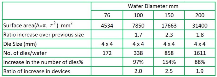
Table 1. The number of die increase with wafer size.
While Tier 1 IDMs have the benefit of fully depreciated and well-optimized day-to-day run yields aiding competitive manufacturing costs and device prices, it will not be so easy for newcomers with 200 mm fabs. These firms will encounter price pressure and lower yield numbers in the near term.The introduction of 200 mm substrates is expected to bring down the overall device cost by 20-35 percent relative to production on a 150 mm platform. This can occur even if there is an increase in material costs at the wafer level. For the ease of achieving good wafer geometry, there is an increase in wafer thickness as the wafer diameter grows. 150 mm-diameter SiC wafers have a thickness of 350 μm, and the initial 200 mm SiC substrates introduced to the market will be 500 μm-thick. As increased thickness reduces the number of wafers made from each puck, there is a slight rise in wafer cost. However, the increased thickness helps to ensure a good wafer geometry, while minimizing bow and warp.
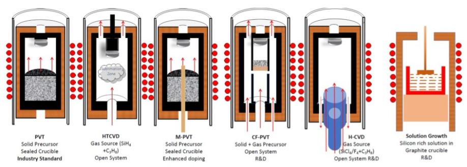
Figure 1. There are several different techniques for producing bulk SiC.
Even with today’s fabrication tooling capabilities, it is possible to produce 350 μm-thick 200 mm wafers that would provide an additional reduction to substrate costs. However, that’s not an essential step, as irrespective of wafer thickness, SiC wafers with a 200 mm diameter offer reduced device costs compared with their 150 mm siblings.While moves to larger substrate sizes over the past two decades have helped to cut production costs for SiC devices, they are still about three times higher than those of silicon variants. That’s not a showstopper, though, because when a circuit designer switches from silicon devices to those made from SiC, they get a 5-10 percent cost reduction at the system level. The introduction of 200 mm SiC wafers will amplify this benefit and lead to further falls in overall system-level cost over the next few years.
Scaling challenges
For elemental semiconductor materials such as silicon and germanium, as well as compound semiconductor materials such as GaAs and InP, crystalline material is grown from the melt. Crystal growers begin by taking a seed crystal, with a cross-section typically 10 mm by 10 mm, and use the thin neck created between the seed and the melt interface to increase the diameter of the crystal to the required level. Once this is established, the crystal is pulled out of the melt at a rate that depends on the material. This rate ranges from 1 mm/hour to 150 mm/hour.
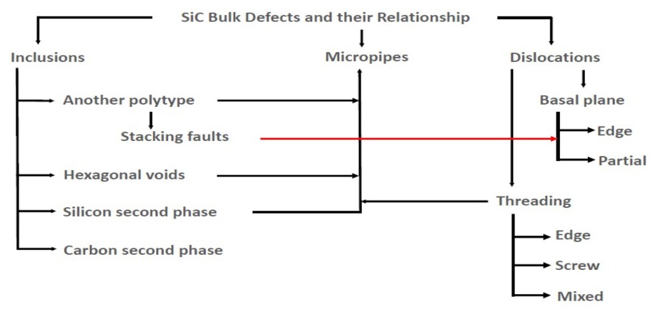
Figure 2. Various defects observed in bulk SiC and their relationship.
One of the biggest downsides of SiC is that the material doesn’t exist in a liquid phase, so crystals can’t be grown from a melt. If SiC is held at a high temperature and low pressure, it dissociates into gaseous species without passing through the liquid phase. Due to this behaviour, SiC crystals are grown using a vapour phase technique called sublimation, or physical vapour transport (PVT). For growing material using this method, an essential ingredient is a seed crystal with a diameter similar to that of the boule (read on to discover how the seeds are expanded). With PVT, growth rates are in the range of 0.1-0.5 mm/hour.To take the quality of SiC to a new high, and to enable a more precise control of the growth of this material, researchers have realized additional advances to the PVT process, and explored other viable options (see Figure 1). One refinement, adopted by industry, is the use of gaseous cracking to supply the carbon and silicon, rather than a solid SiC powder. This technique is called high-temperature chemical vapour deposition (HT-CVD).
Another alternative is modified PVT (M-PVT), an approach that incorporates an additional feed tube into the growth zone for the dopant gas, which could be nitrogen or other materials. This modification enables the production of low-resistivity SiC with uniform resistivity profiles. Using conventional PVT, one downside is that the dopant gas is introduced outside the growth zone. This prevents the production of low-resistivity material with good uniformity, due to limited diffusion.
At the research level, other techniques are being explored for the growth of crystalline SiC. These methods, which are a long way off producing commercial-scale SiC wafers, include halide CVD, as well as a combination of HT-CVD and PVT that is known as continuous-feed PVT.
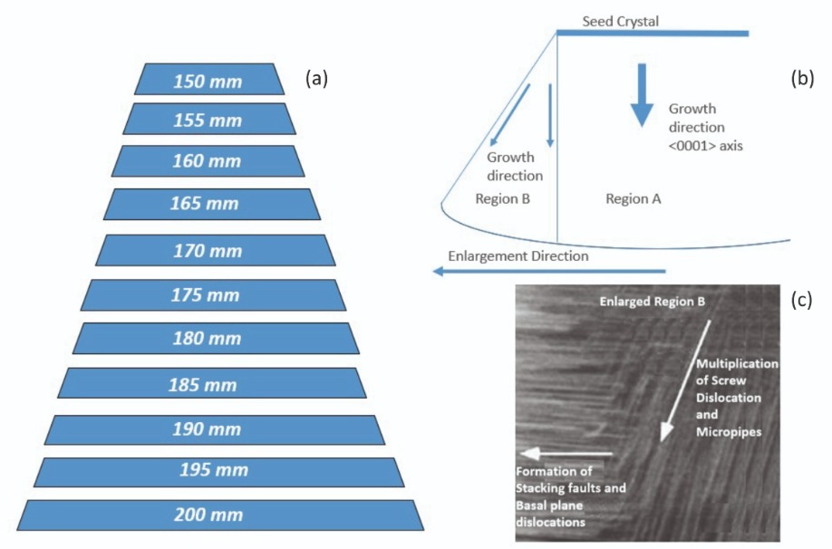
Figure 3. Seed enlargement lies at the heart of the introduction of larger wafer sizes. Shown here are illustrations of: (a) a seed expansion process from 150-200 mm, and (b), the defects that can develop during the seed expansion process. The newly expanded region is susceptible to the formation of more defects (c).
Recently, there has been interest in the growth of bulk SiC from solution, as this has the potential for producing large-sized, high-quality SiC wafers. But this technique, still being researched, is not yet capable of achieving commercialization. One of its drawbacks is that due to the lack of a stoichiometric SiC liquid phase at atmospheric pressure, it is impossible to employ congruent melt growth. Another downside is that the solubility of carbon in molten silicon is very limited at very high temperatures. It is possible to enhance the solubility of carbon by turning to solvents, such as Ti-Si, Al-Si, Cr-Si, Fe-Si, Si-Sc, Si-Co, Sn-Si and Si-Ge. However, these solvents threaten to be incorporated in the grown crystal matrix. Another issue is that the growth of larger crystals is not sustainable with these methods.Due to the considerations surrounding the growth of SiC by a variety of methods, today almost all commercially grown SiC crystals are produced by PVT. With this approach, PVT furnaces are either inductively or resistively heated.
Crystal characteristics
SiC can be crystallized in three crystal structures: cubic (C), hexagonal (H) and rhombohedral (R). Variations of this material are far greater than these three, however, with SiC exhibiting more than 220 polytypes. These differ in how they occupy sites along the c-axis, with classification of the polytype depending on the number of Si-C layers in the unit cell. For power electronic applications, the best polytype is 4H SiC.
Difficulties inherent to vapour phase growth give rise to a variety of defects, including micropipes, screw dislocations, edge dislocations, stacking faults, inclusions, and partial and mixed dislocations. Device performance is impaired by micropipes, screw dislocations and basal planar defects. However, the density of these imperfections can be reduced during crystal growth and subsequent epilayer deposition, which takes place prior to front-end processing. The relationship between the different defects in SiC is illustrated in Figure 2.
During the past twenty years, manufacturers of SiC have taken a step-by-step approach to expanding seed sizes. Progress is not easy, as this expansion is a time-consuming, iterative process, involving several cycles of learning and process optimization. The starting point for seed development dates back to the 1990s, with the formation of self-nucleated Lely platelets with a 4 mm by 4 mm cross-section.
These days, efforts are directed towards expanding seeds from 150 mm to 200 mm, a challenging task given that the newly expanded region is susceptible to the formation of more defects (see Figure 3). Success in expanding seed dimensions demands a concurrent undertaking of several iterations of thermal and crystal growth computation, fluid dynamics and numerical modelling in a virtual platform, and hot zone design optimization for larger seed sizes. To preserve the quality of the crystal in the starting seed, there is a need to control the advancement of the solid-gas interface and maintain the shape of the growth interface via careful selection of axial and radial temperature gradients.
Evaluating economics
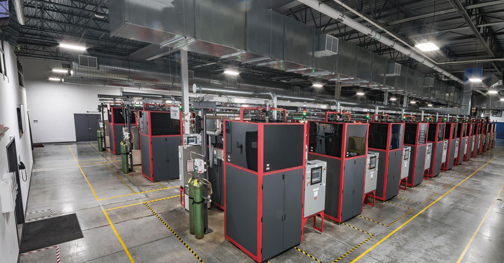
With the growth rate for 200 mm SiC crystals almost the same as that for their 150 mm siblings, there is no appreciable increase in the production cycle time, allowing equipment throughput to be maintained. Costs do rise slightly, however, due to an increase in the expense of hot-zone components, stemming from an increase in the size of this part in the growth chamber. Fortunately, there have been recent advances in graphite manufacturing, as well as a far better understanding of how to tune the growth process. Due to these gains, it is now viable to make cost-effective hot-zone components for 200 mm crystal growth, and if higher volumes are used, expenditure diminishes. Working in this manner, our team at GT Advanced Technologies (GTAT) has developed the SiClone 200 platform, which is capable of producing 150 mm and 200 mm diameter crystals without additional capex.

Figure 4. GTAT’s progress in crystal growth from 50 mm to 200 mm.
As well as crystal growth, seed/wafer fabrication involves outer diameter grinding, flat grinding, wafering, lapping and polishing – and each process needs to be optimized as the wafer diameter increases. There are already productivity increases at the wafering step, accomplished by reducing kerf loss during the slicing process. Traditionally, slicing SiC wafers involves multi-wire saws and diamond slurry, and leads to a kerf loss below 200 μm and a grinding loss of less than 100 μm, required for removal of sub-surface damage. Introducing laser-based slicing trims total material losses for wafer processing by one-third, to around 100 μm.
At the fab level, cost increases associated with migrating to 200 mm are minimal. Offsetting the relatively low add-on costs for 200 mm SiC crystal growth and wafer manufacturing is an increase in the number of dies per wafer. This makes the switch, which will deliver significant dividends in the power electronic industry, profitable and sustainable. Today’s epi-ready 150 mm SiC wafers retail for $750-$900, and 200 mm wafers are expected to be priced at $1300-$1800. At GTAT, we have a roadmap to reduce costs even further.
Our company has a rich heritage as a manufacturer of crystal growth furnaces, with a global installed base of thousands of systems, and a strong track record in increasing wafer diameters (see Figure 4). Our know-how in equipment design, process scaling, facility planning, and the supply chain helps us to ramp SiC capacity faster, while competing successfully on price and quality. We are now in a position to push forward with 200 mm SiC, thanks to our continuous improvement, grounded in increased cycles of learning and optimization, along with R&D efforts. Our 200 mm product launch is slated for late 2021/early 2022.
If SiC continues to follow in the footsteps of the silicon industry, the next wafer size could be 300 mm. According to our initial thermal modelling, implementing unique hot-zone design components could minimize the applied shear stress, which is responsible for generating dislocations and micropipes, along with the von Mises stress that is to blame for boule cracking. If, further down the line, the industry seeks a 300 mm SiC wafer to reduce costs, we are confident in our ability to develop that next-generation crystal.
Acknowledgements
The author profoundly thanks his colleagues and the world-class manufacturing team at GTAT. Special thanks and sincere appreciation to GTAT colleagues Chris Van Veen, Henry Chou and Jeff Gum, and Simon Price of Exawatt for useful discussions and critical review.


