Refining the multi-junction solar cell

The Roll Out Solar Array has been used on the International Space Station. Credit: Boeing.
Multi-junction cells continue to improve by offering greater flexibility, a path towards streamlined manufacture and falling production costs
BY RICHARD STEVENSON
MANY DIFFERENT MATERIALS are competing in the solar market. For solar farms and rooftops, silicon dominates, providing rock-bottom prices for electrical generation. Cells made from a stack of compound semiconductor materials can’t compete on this key metric, even when operating under very high levels of concentration and delivering far higher efficiencies.
Up in space and powering a satellite priorities are very different, playing into the hands of multi-junction cells featuring compound semiconductors. While cost still matters, it is only one of several important factors, and a premium is placed on efficiency. Excelling in this regard allows more power to be generated, and ultimately enables either the technologies on board to perform more tasks, or for actions to be undertaken that require more energy, such as electrical propulsion. Alternatively, gains in efficiency enable a reduction in cell area for the same power generation, leading to smaller satellites and lower launch costs.
Another attribute of the multi-junction cell is its superior radiation hardness. In space, cells are bombarded by high-energy protons and electrons, causing severe damage to devices that reduces their output. All cells suffer, but III-Vs less so than silicon, the previous incumbent in this domain. This means that the fall in efficiency of these triple-junction cells over the duration of a mission is relatively small.
For more than two decades, power generation in space has been dominated by these high-efficiency cells, which typically combine a junction made from germanium with two or more based on GaAs and GaInP. Over that time much effort has been devoted to increasing the efficiency of the device, which has climbed steadily. But that’s not the only improvement that’s been made. As highlighted in talks delivered at this year’s European Photovoltaic Solar Energy Conference and Exhibition (EU PVSEC), held on-line from 6-10 September, progress is being made in cutting manufacturing costs through the use of larger substrates and different foundations, and producing flexible cells that drive down launch costs.
Favouring flexibility
In Europe, flexible multi-junction cells, formed via substrate removal, are being developed through a multi-partner project entitled ALFAMA – that’s short for Advanced Lightweight and Flexible Array with Mechanical Architecture. At EU PVSEC Jonas Schön from Fraunhofer ISE detailed some of the progress to date in this effort that is backed by Ä3 million of funding and involves many partners, including Airbus, Azur Space Solar Power and tf2 devices.
_(4)-svhm91.jpg)
Flexible solar cells are needed on the ROSA (Roll Out Solar Array) held by the robotic arms at the International Space Station.

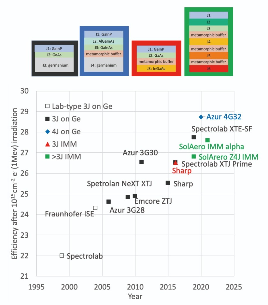
Figure 1. To evaluate the performance of multi-junction cells in space, it is appropriate to consider the efficiency after bombardment by radiation. It is common practice to use the condition of bombarded by 1015 electrons/cm2 with an energy of 1 MeV. The use of an inverted metamorphic (IMM) structure allows the device to provide flexibility.
The ALFAMA project will help to drive flexible cells forward, with efforts directed at realising a power-to-mass ratio of greater than 1.3 Watts/gram. That’s roughly a factor of two compared with a state-of-the-art conventional solar cell, according to Schön, who explained that another target of the project is to break new ground for the thinness of the cell. This will be trimmed below 40 μm. Progress on both these fronts will be made using low-cost manufacturing processes.
Before detailing the device adopted in the project, Schön reviewed several different forms of multi-junction cell that have been used in space. He explained that during the last two decades, efficiencies for devices with the relatively simple, conventional design that features a germanium bottom cell have made steady progress. Over this timeframe, efficiencies have climbed from around 24 percent to almost 28 percent, according to measurements on cells that have been bombarded by 1015 electrons/cm2 with an energy of 1 MeV to mimic the impact of radiation in space (see Figure 1). “The drawback [with this design], apart from the non-perfect efficiency, is the thickness due to the germanium substrates,” remarked Schön.
He pointed out that one option for reaching higher efficiencies is to add another junction, citing the 4G32 from Azur as an example. This product includes a metamorphic buffer to overcome lattice mismatch between the germanium sub-cell and the three III-V sub-cells. This design is able to reach an end-of-life efficiency of nearly 29 percent, but is still impaired by the thickness of the germanium substrate.
Overcoming this issue are the inverted metamorphic triple-junction cells, which employ GaAs, InGaP and InGaAs sub-cells. “These solar cells are potentially lightweight and flexible, but a little bit less radiation hard. Nevertheless, the solar cell from Sharp reaches an end-of-life efficiency comparable to other triple junction cells on germanium.” SolAero is also pursuing this approach, and has produced devices with up to six junctions that are just shy of an efficiency of 28 percent (see Figure 1).
A triple-junction version of the inverted metamorphic has been used in the ALFAMA project. Efforts involved taking a GaAs substrate and depositing a release layer, followed by a 1.9 eV GaInP sub-cell, a 1.4 eV GaAs sub-cell, a metamorphic buffer and a 1.0 eV GaInAs sub-cell. Engineers at tf2 devices removed the release layer by etching, before inverting the structure and adding: an anti-reflection coating and contact to the top of the device; and a metal to the bottom, which provides an electrical contact and aids structural integrity. In principal, the GaAs substrate can be re-used.
The team compared the performance of their device with a standard triple-junction cell. For this control, which has a cell size of 20 cm2 and a total epitaxial thickness of around 10 μm, the areal density is 13.2 mg/cm2 and the beginning of life efficiency 26 percent. Efficiency did not degrade during thermal cycling, undertaken to mimic conditions onboard a satellite.
Turning to simulations allowed the team to optimise their structure for different radiation doses. Insights provided by these calculations included the benefits of increasing doping in the contact layers, which improves efficiency through increases in the fill factor and the open-circuit voltage. Following irradiation, cells have produced an efficiency of 25.4 percent and an impressive power-to-mass ratio of 2.6 Watt/gram.
Schön and co-workers used electroluminescence to evaluate the performance of all three sub-cells. They found the material quality in the InGaP and InGaAs cells inferior to GaAs, due to the thermal load and the impact of the metamorphic buffer, respectively.
For the latest generation of cells, improvements were made to thin-film processing, current matching and the anti-reflection coating. Devices had a beginning-of-life efficiency of 30.2 percent.
The power-to weight ratio of the multi-junction cells produced by the project are similar to those of devices made by Sharp and Microlink, formed using a process involving separation of the device from the substrate. For the ALFAMA project, there is a particularly encouraging performance at the beginning of life. “For end-of-life we are optimistic that we will reach the efficiency of the Sharp cell in the near future.”
Scaling germanium
Within the semiconductor industry, a well-worn path to increasing productivity and trimming production costs is to increase the size of the wafer. Recently, Umicore has enabled the III-V solar industry to take another step on this road by offering 200 mm germanium. Investigating this opportunity is Azur Space Solar Power, which has been evaluating the growth of triple-junction cells on this platform through an EU-funded project entitled RadHard.
Details of its findings were unveiled to delegates in a talk delivered by Tim Kubera from Azur. He explained that the company has established production of triple-junction devices with an efficiency of around 30 percent on 100 mm and 150 mm germanium substrates. MOCVD reactors can routinely accomodate twelve 100 mm wafers or eight 150 mm wafers. However, for the RadHard project the team is using an MOCVD reactor that houses five 200 mm wafers. “By increasing the format we can process more area per run, which should result in cost benefits,” said Kubera.

Table 1. Through the RadHard project, a team of engineers in Europe have made 60 cells with a size of 30.18 cm2 from 19 wafers with a 200 mm diameter. A high shunt resistance and a scratch led to the discarding of two cells. Electrical performance is determined from current-light-voltage plots using an AM0 spectrum. Isc is the short circuit current; Voc the open-circuit voltage; Imp, Vmp and Pmp the maximum values for current, voltage and power, respectively; FF is the fill factor; and h the cell efficiency.
A range of metrology techniques have been used to evaluate, across the wafer, the quality of multi-junction epitaxial stacks grown on 150 mm and 200 mm germanium. Growth rates have been determined by a combination of in-situ measurements and a profilometer; X-ray diffraction has provided an insight into material quality; and capacitance-voltage plots have tracked doping levels. Analysis of the GaInP top cell indicates that shifting to a larger wafer has little impact on the profiles associated with growth rate and composition. “The only real discrepancy we see is in the relative doping,” revealed Kubera. “For the bigger wafers, the emitter doping of the top cell is shown to increase by up to 25 percent at the outer edge.” Smaller variations have been observed in key characteristics of the InGaAs region, the Bragg materials and the InAlP window layer.
While this could be improved, it has not prevented the team from assessing the quality of devices produced from the larger foundation. As they are yet to have access to a 200 mm line, they have used a laser process to extract a pair of 100 mm wafers from the 200 mm wafer. This standard size allows the use of an established 4x8 cell design.
Adopting this approach, the team fabricated 60 cells, using nineteen 200 mm wafers from four epi-runs. Measurement on 58 cells showed very little variation between them (see Table 1). The other two cells, both with an efficiency below 29 percent, were discarded; one suffered from a shunt resistance and the other a big scratch.

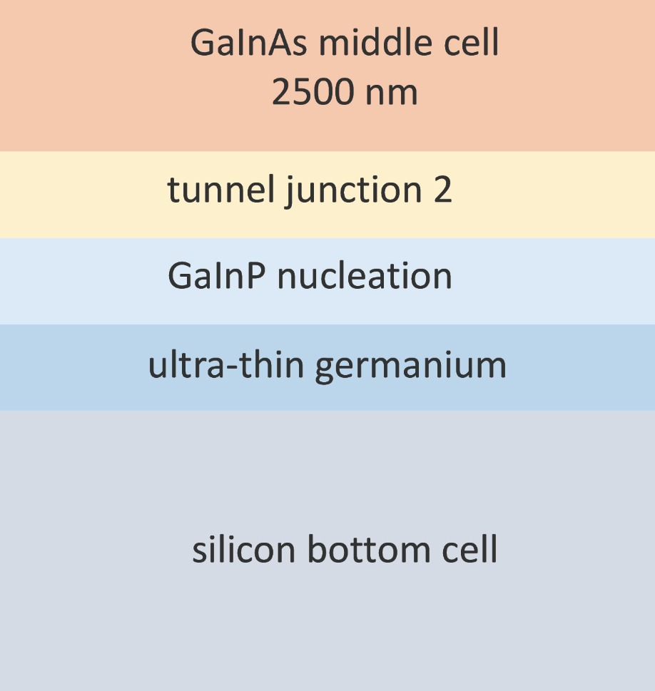
Figure 2. Test structures suggest that an ultra-thin layer of germanium, deposited by RF plasma-enhanced CVD, could enable the production of multi-junction cells on silicon substrates.
Virtual value
An alternative option for scaling that promises large wafers, while realising low costs that might allow multi-junction cells to be used for terrestrial power generation, is to grow germanium and III-V layers on silicon substrates. It’s an approach that has been pursued for several years by a team from The Technical University of Madrid, with recent efforts shifting to thinner germanium layers.
At this year’s EU PVSEC a spokesman for this group, Iván García, provided an overview of the recent work, undertaken in collaboration with researchers at LPICM-CNRS in Palaiseau, France.
Placing the latest work in context, Garcia explained that the team had previously investigated the fabrication of triple-junction cells on silicon that had a germanium layer acting as a low energy sub-cell. The epiwafers were plagued with cracking, due to a difference in the thermal expansion coefficient, exacerbated by the 2-5 μm-thick germanium layer.
Garcia explained that to reduce cracking, they now stay below the critical thickness, having reduced the total thickness for the epistack from 10 μm to 5.5 μm. The first attempts with the new structure produced promising results, but uncovered some issues. On the plus side, the team found that the short-circuit current approached that for a conventional triple-junction cell grown on germanium. However, metastability still plagued the heterostructure, with the thinner structure failing to deliver an improvement in the open-circuit voltage, due to the use of templates with a high threading dislocation density.
To overcome that issue, the team is now using a low-temperature RF plasma-enhanced CVD process, developed by those of the group in France, to deposit ultra-thin germanium layers. “They have achieved high-quality epitaxial layers at temperatures as low as 175 degrees [Celcius],” explained Garcia. “We think this is an advantage, because the lower-temperature processes can be lower cost than higher temperature processes.” Using this approach, involving germanium layers with a thickness in the range 20-140 nm, threading dislocation densities can be as low as 5 x 106 cm-2.
One consequence of switching to ultra-thin germanium layers is that they can no longer be used for the low-energy sub-cell. So silicon is employed for the bottom junction. It is a compromise, offering simple low-cost fabrication steps, but the bandgap for the bottom cell is not ideal for terrestrial spectra. What’s more, light is absorbed in the geranium layer, reducing the current produced by the silicon sub-cell.
Modelling by the team has determined, for a range of thicknesses for the germanium layer, how thick each of the top two junctions should be to maximise efficiency. “These thicknesses are way below the thicknesses for cracking, which is good,” enthused Garcia, who explained that to maximise the performance from the silicon sub-cell, there needs to be back passivation and the introduction of light-trapping technologies.
An alternative approach to increasing efficiency is to increase the bandgap of the top two sub-cells by switching to AlInGaP and AlGaAs. According to modelling, the aluminium content can be below 10 percent, leading Garcia to believe that it should be possible to produce high-quality junctions.
Modelling a range of triple-junction cells with different bandgaps and threading dislocation densities suggests that for a germanium thickness below 60 nm, efficiencies of 30-34 percent under 1 sun are attainable.
“This potential efficiency is less than that obtainable by other techniques, such as wafer bonding, but we think that the simplicity of this method could be worth it,” argued Garcia.
To start investigating whether this approach can fulfil its promise, the team produced a tandem cell featuring a germanium layer just 20 nm thick (see Figure 2). These efforts were compromised by: a lack of optimisation of the silicon surface prior to growth; a high threading dislocation density of the template; no back surface passivation in the silicon cell; and impurity in-diffusion, occurring during MOCVD growth of the upper layers. However, despite all this, for some incident wavelengths the device could still produce its target efficiency.
The team is now building on this promising start by using plasma etching to improve the surface of the silicon wafer, and developing techniques to trim the dislocation density, aided by analysis of the interface between silicon and germanium.
Progress on this front, along with that on larger substrates and an increasing number of flexible designs, will increase the prowess of the multi-junction cell. It shows no sign of loosening its vice-like grip
on powering satellites, and if chip costs fall, that will improve its chances of generating terrestrial energy.


