
Advanced III-V-on-silicon photonics
Scientists from Hewlett Packard Labs in Milpitas review the latest advances in III-V-on-silicon integration
In a new review article publication from Opto-Electronic Advances, scientists from Hewlett Packard Labs in Milpitas discuss advanced III-V-on-silicon photonic integration.
Among various integration methods, heterogeneously integrating III-V material onto silicon substrate by using wafer bonding technology is the most popular one and is currently appearing in commercial products. Direct epitaxial growth of III-V layers on silicon, on the other hand, also has huge research interest due to its potential as a solution for very high density integration in the long term.
In addition, a newly emerged III-V-on-silicon photonic integration method by epitaxial regrowth III-V material on a bonded substrate has attracted a lot of interest.
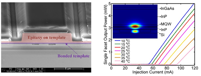
Research groups from Hewlett Packard Labs, III-V labs and Sophia University have invested in this advanced integration method and demonstrated their working lasers separately. By creating a native template on silicon substrate by using wafer bonding technology, lattice-matched epitaxy can be conducted accordingly on the template. This advanced integration method aims to providing high quality III-V-on-silicon photonic integration by benefit from both direct epitaxy and wafer bonding technologies.
In this article, researchers from Hewlett Packard Labs review recent research work on this integration platform of regrowth on bonded template from various research groups. With the investigations of the similarities and differences of template developments, comparisons and analysis of the epitaxial regrowth and fabricated laser devices, growing interest and huge potential in this novel concept of regrowth on bonded template have been present.
Further discussions have indicated that this method has many potential advantages such as it provides high-quality laser material on Si substrate, and it is cost competitive over other existing III-V-on-silicon integration approaches. Particularly, except the great practicality for on-chip light source and other functional devices for Si photonics, researchers from Hewlett Packard Labs believes that this integration concept is a general approach for combining different materials onto various substrates.
'An advanced III-V-on-silicon photonic integration platform' by Hu YT, Liang D, Beausoleil RG; Opto-Electron Adv 4, 200094 (2021)


