Diminishing droop with multi-junction LEDs

MOCVD-grown LEDs with multiple tunnel junctions push peak efficiency to higher drive currents
A collaboration between researchers at The Ohio State University and Sandia National Labs is claiming to have produced the first triple-junction LEDs grown by MOCVD. According to the team, their work shows that with proper tunnel-junction design it is possible to increase wall-plug efficiency at high output powers by cascading several nitride-based LEDs.
This advance could improve the performance of high-power LEDs deployed in domestic, industrial and automotive lighting. While droop has been reduced in LEDs used for these applications, it is still an issue.
“We have been informed by those in the LED industry that fixing droop remains a significant challenge that they are actively pursuing, especially in longer wavelength LEDs,” revealed team spokesman Zane Jamal-Eddine.
The recent success by the US collaboration is underpinned by a breakthrough in tunnel-junction design reported earlier this year. Simulations forming part of that previous work showed that the voltage penalty across MOCVD-grown tunnel-junction LEDs can be minimised by carefully controlling the doping profile. Optimising the magnesium profile in the heavily-doped p-type layer is particularly important. “Furthermore, it is key to utilise polarization charge to provide a favourable electric field profile to enhance the tunnelling probability,” added Jamal-Eddine.
The team accomplished all these objectives by including a heavily doped, graded InGaN region with a peak composition of 6 percent indium in the tunnel-junction. The resulting three-dimensional polarization charge helps to compensate for doping issues associated with MOCVD grown tunnel-junctions, which tend to cause them to have a much higher forward voltage than equivalents grown by MBE.
Thanks to the introduction of the polarization charge, alongside optimisation of the doping profile, the forward voltage across the team’s MOCVD-grown tunnel-junctions is similar to those grown by MBE. “This enabled the improvement in forward voltage, external quantum efficiency, and wall-plug efficiency scaling that we observed in our dual- and triple-junction cascaded LEDs,” remarked Jamal-Eddine.
He and his co-workers produced their devices using a Taiyo Nippon Sanso SR4000HT reactor. Underpinning the device structure, formed on sapphire substrates, is: a 6 μm-thick layer of n-type GaN with a dislocation density of around 108 cm-2; a 500 nm-thick n-type GaN layer doped with silicon to a level of 5 x 1018 cm-3; and a 190 nm-thick In0.04Ga0.96N underlayer, incorporated to prevent formation of V-type defects. On this platform the team produced LEDs with one, two and three junctions. Etching followed to create 100 μm by 100 μm mesas, before rapid thermal annealing activated the carriers in the buried p-type GaN layers.
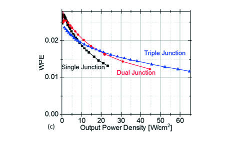
Electrical measurements on devices with a ring-shaped top n-type contact showed that the turn-on voltage increased from 3.3 V for the single-junction device to 6.9 V and 10.8 V for double- and triple-junction variants. Electroluminescence measurements revealed that the peak of the external quantum efficiency scaled by 200 percent with the introduction a two-junction device, and 275 percent with a three-junction device (see figure above). These significant increases demonstrate that multi-active regions allow LEDs to offer a better performance at higher powers.
Moving to even more junctions promises to push peak efficiency to an even higher drive current, but there are concerns over degradation of underlying layers, associated with the thermal budget. Another issue in these structures is the propagation of extended defects, formed in the heavily-doped tunnel-junction layers. The team have hunted for these defects with a transmission electron microscope, but have found no evidence for them.
Jamal-Eddine says that the team are currently looking into possible thermal budget issues to see if they can push the device any further, or to a larger number of junctions.
Reference
Z. Jamal-Eddine et al. Appl. Phys. Express 14 092003 (2021)


