Loading...
News Article

Directional management of perovskite defects

News

Chinese team passivate perovskite solar cell interface defects using new-type of low-dimensional perovskite

Perovskite solar cells show great application prospects. However, a large number of unfavourable defects, growing up after or during annealing process due to their ionic nature, lead to sites of nonradiative recombination and accelerate degradation of device efficiency and stability.

A research team lead by Pan Xu from Hefei Institutes of Physical Science (HFIPS), cooperated with Zheng Haiying from Anhui University, achieved high-efficiency perovskite solar cells by passivating interface defects using new-type low-dimensional perovskite.The work been published on ACS Energy Letters.

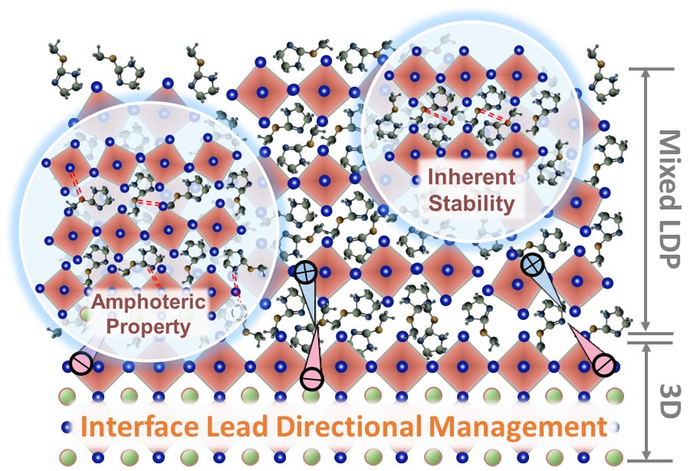
This team passivated and stabilised the perovskite light absorbing layer with amphoteric heterocyclic cation, and designed a new-type low-dimensional perovskite passivation layer. This novel perovskite could deal with different surface-terminating ends at the interface and show multiple passivation effects owing to its amphoteric nature and strong molecular interaction.

According to the theoretical calculation of defect formation energy, the formation of lead-based defect was effectively inhibited. The modified perovskite solar cells displayed reduced defect density and lowered nonradiative recombination, thereby leading to the power conversion efficiency exceeded 24 percent. Besides, the long-term stability against humidity, high temperature and light was improved.

This work indicated a direction for the directional management of interface Pb-based defects during the practical application of perovskite photovoltaic devices.

'Mixed-Phase Low-Dimensional Perovskite-Assisted Interfacial Lead Directional Management for Stable Perovskite Solar Cells with Efficiency over 24 percent' by

Guozhen Liu et al; ACS Energy Letters 2021

SiC MOSFETs: Understanding the benefits of plasma nitridation
Wolfspeed reports Q2 results
VueReal secures $40.5m to scale MicroSolid printing
Mitsubishi joins Horizon Europe's FLAGCHIP project
Vishay launches new high voltage SiC diodes
UK team leads diamond-FET breakthrough
GaN adoption at tipping point, says Infineon
BluGlass files tuneable GaN laser patents
QD company Quantum Science expands into new facility
Innoscience files lawsuit against Infineon
Riber revenues up 5% to €41.2m
Forvia Hella to use CoolSiC for next generation charging
Photon Design to exhibit QD simulation tool
Ortel transfers CW laser fabrication to Canada
Luminus adds red and blue multi-mode Lasers
PseudolithIC raises $6M for heterogeneous chiplet tech
Mesa sidewall design improves HV DUV LEDs
IQE revenue to exceed expectations
'Game-changing' VCSEL system targets clinical imaging
German start-up secures finance for SiC processing tech
Macom signs preliminaries for CHIPS Act funding
IQE and Quintessent partner on QD lasers for AI
EU funds perovskite tandems for fuel-free space propulsion
EU to invest €3m in GeSi quantum project
Transforming the current density of AlN Schottky barrier diodes
Turbocharging the GaN MOSFET with a HfOâ‚‚ gate
Wolfspeed launches Gen 4 SiC MOSFET technology
Report predicts high growth for UK's North East
Element Six unveils Cu-diamond composite
SemiQ launches hi-rel 1700V SiC MOSFETs
Lynred to exhibit Eyesential SWIR sensor for machine vision
Thorlabs buys VCSEL firm Praevium Research
×
Search the news archive

To close this popup you can press escape or click the close icon.
Logo
x
Logo
×
Register - Step 1

You may choose to subscribe to the Compound Semiconductor Magazine, the Compound Semiconductor Newsletter, or both. You may also request additional information if required, before submitting your application.


Please subscribe me to:


You chose the industry type of "Other"

Please enter the industry that you work in: