
Scientists make stable, high mobility ITZO TFTs
Tokyo Tech team shows cheaper way forward for next-generation display technologies
The trade-off between carrier mobility and stability in amorphous oxide semiconductor-based TFTs has been finally overcome by researchers from Tokyo Institute of Technology (Tokyo Tech) in an ingeniously fabricated indium tin zinc oxide TFT. This could pave the way for the design of display technologies that are cheaper than current silicon-based technologies.
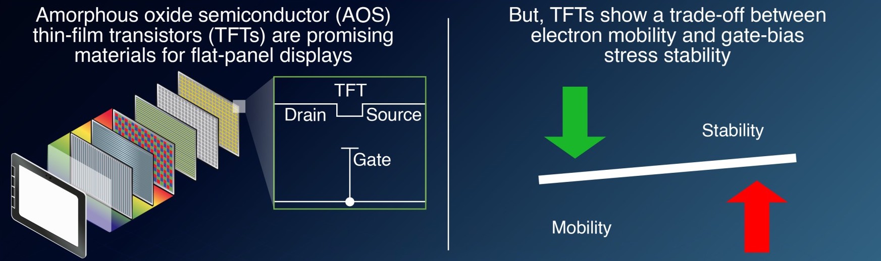
Amorphous oxide semiconductors (AOS) are a promising option for the next generation of display technologies due to their low costs and high electron (charge carrier) mobility. The high mobility, in particular, is essential for high-speed images. But AOSs also have a distinct drawback that is hampering their commercialization — the mobility–stability tradeoff.
One of the core tests of stability in TFTs is the “negative-bias temperature stress” (NBTS) stability test. Two AOS TFTs of interest are indium gallium zinc oxide (IGZO) and indium tin zinc oxide (ITZO). IGZO TFTs have high NBTS stability but poor mobility while ITZO TFTs have the opposite characteristics. The existence of this tradeoff is well-known, but thus far there has been no understanding of why it occurs.
In a recent study published in Nature Electronics, a team of scientists from Japan have now reported a solution to this tradeoff. “In our study, we focused on NBTS stability which is conventionally explained using ‘charge trapping.’ This describes the loss of accumulated charge into the underlying substrate. However, we doubted if this could explain the differences we see in IGZO and ITZO TFTs, so instead we focused on the possibility of a change in carrier density or Fermi level shift in the AOS itself,” explains assistant professor Junghwan Kim of Tokyo Tech, who headed the study.
To investigate the NBTS stability, the team used a “bottom-gate TFT with a bilayer active-channel structure” comprising an NBTS-stable AOS (IGZO) layer and an NBTS-unstable AOS (ITZO) layer. They then characterized the TFT and compared the results with device simulations performed using the charge-trapping and the Fermi-level shift models.
They found that the experimental data agreed with the Fermi-level shift model. “Once we had this information, the next question was, ‘What is the major factor controlling mobility in AOSs?’” says Kim.
The fabrication of AOS TFTs introduces impurities, including carbon monoxide (CO), into the TFT, especially in the ITZO case. The team found that charge transfer was occurring between the AOSs and the unintended impurities. In this case the CO impurities were donating electrons into the active layer of the TFT, which caused the Fermi-level shift and NBTS instability. “The mechanism of this CO-based electron donation is dependent on the location of the conduction band minimum, which is why you see it in high-mobility TFTs such as ITZO but not in IGZO,” elaborates Kim.
Armed with this knowledge, the researchers developed an ITZO TFT without CO impurities by treating the TFT at 400°C and found that it was NBTS stable. “Super-high vision technologies need TFTs with an electron mobility above 40 cm2 (Vs)-1. By eliminating the CO impurities, we were able to fabricate an ITZO TFT with a mobility as high as 70 cm2 (Vs)-1,” comments Kim.
However, CO impurities alone do not cause instability. “Any impurity that induces a charge transfer with AOSs can cause gate-bias instability. To achieve high-mobility oxide TFTs, we need contributions from the industrial side to clarify all possible origins for impurities,” says Kim.
The results could pave the way for fabrication of other similar AOS TFTs for use in display technologies, as well as chip input/output devices, image sensors and power systems. Moreover, given their low cost, they might even replace more expensive silicon-based technologies.
Reference
Shiah, YS., Sim, K., Shi, Y. et al. Mobility–stability trade-off in oxide thin-film transistors. Nat Electron 4, 800–807 (2021)


