
Gallium oxide SBD breakthrough
Novel Crystal Technology develops world's first ampere-class 1200V breakdown-voltage gallium oxide Schottky barrier diode
Japanese firm Novel Crystal Technology, which is working on the commercial development of β-Ga2O3 Schottky barrier diodes as part of NEDO’s 'Strategic Energy Conservation Technology Innovation Program', has announced an ampere-class 1200V breakdown-voltage Schottky barrier diode (SBD).
The company says this achievement will greatly advance the commercialisation of gallium oxide SBDs with high breakdown voltages and will lead to lower priced and higher performance power electronics.
In addition, by enabling more efficient and miniaturised power electronics devices such as power converters for photovoltaic power generation, general-purpose inverters for industrial use, and power supplies, this SBD is expected to contribute to the efficient use of electric energy such as through electrification of automobiles and flying cars. The details of this achievement were published in the online version of Applied Physics Express published by the Japan Society of Applied Physics on December 15, 2021.
β-Ga2O3 has superior material properties and has a less costly crystal growth method than that of SiC or GaN, which are competing high-performance materials to replace silicon. Low-loss, low-cost power devices can be made from β-Ga2O3, and it is expected that they can be used in home appliances, electric vehicles, railway vehicles, industrial equipment, solar power generators, and wind power generators. Research and development on β-Ga2O3 is accelerating at domestic and overseas companies and research institutes with the goal of using this material to miniaturise and improve the efficiency of electrical equipment.
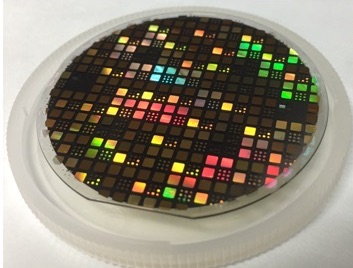
Novel Crystal Technology embarked on its plan to commercialise β-Ga2O3devices in 2017, and it has been working on demonstrating β-Ga2O3 Schottky barrier diodes (SBDs) as part of the Strategic Energy Conservation Technology Innovation Program of the New Energy and Industrial Technology Development Organisation (NEDO). Using our research prototype line and a foundry, we have developed a mass-production process for trench-type β-Ga2O3 SBDs on 2-inch wafers and have developed the first ampere-class 1200V breakdown-voltage β-Ga2O3. It is expected that high-voltage β-Ga2O3 SBDs arising from this development will have applications such as next-generation quick chargers, for which the need for higher voltage and higher power will increase in the future.
There is a substantial history behind this achievement. Tamura Corporation, the parent company of Novel Crystal Technology, succeeded in developing the world’s first β-Ga2O3 epitaxial wafers for power devices in 2015 through its participation in a NEDO-funded project, 'Strategic Energy Conservation Technology Innovation Program / Research and development of ultra-high voltage gallium oxide power device', from 2011 to 2013.
Since 2018, the company has been developing practical β-Ga2O3 SBDs for power devices in the NEDO-funded project, 'Strategic Energy Conservation Technology Innovation Program / Research and development of ampere-grade gallium oxide power device'. The success reported here is based on the results of another NEDO-funded project, 'Strategic Energy Conservation Technology Innovation Program / Commercial development of β-Ga2O3 SBD”'that Novel Crystal Technology has been participating in since 2020. The details of this achievement were published in the online version of Applied Physics Express published by the Japan Society of Applied Physics on December 15, 2021.
Achievements

Until now, the planar type structure, which is relatively easy to process, has been used for high-current β-Ga2O3 SBDs. However, since the planar type has a large leakage current, it is difficult to manufacture a planar β-Ga2O3 SBD with a breakdown voltage of 1200V. In 2017, Novel Crystal Technology, Inc. succeeded in demonstrating a trench-type β-Ga2O3 SBD that reduces reverse leakage current to 1/1000, and since then, it has been improving the device’s breakdown voltage and increasing the current.
The diagram above is an optical image and a schematic cross-section of the developed β-Ga2O3 field-plated trench MOSSBD. The device has a forward current IF of 2 A (VF = 2.0 V) (Fig. 2a below), breakdown voltage of 1200 V, and low leakage current <10-9 A (Fig. 2b below). At present, the company is able to mass produce SBDs on 2-inch wafers by using a research prototype line and a foundry.

Figure 2. Current-voltage characteristics of the developed β-Ga2O3 field-plated trench MOSSBD
Future plans
Through its participation in NEDO projects, Novel Crystal Technology will establish the manufacturing process and ensure the reliability of these new 1200V breakdown-voltage β-Ga2O3 SBDs, aiming for commercialisation in 2023. The company will also build a 100-mm mass-production foundry line for high-quality β-Ga2O3 100-mm epitaxial wafers, which started to go on sale in June 2021.
The market for medium- and high-voltage high-speed diodes, which is expected to expand to 120 billion yen in 2022 and 150 billion yen by 2030 would especially benefit from this development.


