HVPE yields vertical GaN p-n diodes

A new approach for magnesium-doping enables the continuous growth of vertical GaN p-n diodes by HVPE
Engineers at Nagoya University, Japan, are claiming to have produced the first GaN p-n diodes by HVPE, a technique that combines very high-growth rates with carbon-free sources.
Spokesman for the team, Kazuki Ohnishi, says that this work could cut production costs for vertical GaN power devices, due to the switch from MOCVD to HVPE. “According to our estimates, manufacturing 400 million 6-inch epiwafers will cost $530 billion with MOCVD, but can be reduced to $76 billion with HVPE.”
At present, companies ordering HVPE reactors are offered bespoke tools, primarily for research. However, if demand rises, due to greater interest in this growth technique, it could drive the development of reactors for high-volume production.
It is also possible to produce GaN p-n diodes by growing the n-type region by HVPE, followed by the p-type layers by MOCVD. However, the downside of that hybrid approach is that it tends to create silicon impurities at the interface – and they result in poor electrical properties for the diode. By employing continuous HVPE growth, Ohnishi and co-workers avoid creating silicon-accumulating layers at the p+-n interface.
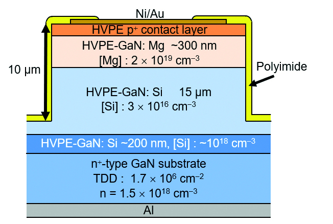
The team from Nagoya produced its devices on a free-standing, HVPE-grown GaN substrate with a threading dislocation density of 1.7 x 106 cm-2 and a carrier concentration of 1.5 x 1018 cm-3. On this foundation they first deposited, by HVPE, a pair of silicon-doped n-type layers – initially a 200 nm-thick n+ layer, and then a 15 µm-thick n-type layer, grown at 30 µm/hour, with a silicon concentration of 3 x 1016 cm-3. For the p-side they added a 300 nm-thick GaN layer with a magnesium doping concentration of 2 x 1019 cm-3, and a 20 nm-thick GaN contact layer, heavily doped with magnesium.
Crucial to the team’s pioneering of HVPE growth of vertical GaN p-n diodes has been the development of a new approach to magnesium doping. As far back as the 1970s, researchers had realised p-doping in HVPE-grown films using magnesium. However, the high equilibrium vapour pressure of the metal source hampered control of the doping level.
Ohnishi and colleagues have addressed this weakness by switching the magnesium source to MgO, which has a very low equilibrium vapour pressure and a melting point of 2800 °C. The new process involves supplying HCl gas to heated MgO. A reaction results in MgCl2, a precursor for the growth process.One concern with this approach is that MgO could introduce oxygen impurities. However, this does not appear to be an issue, according to Ohnishi: “Fortunately, the oxygen concentration is suppressed, even if magnesium oxide is used. This mechanism is under investigation, but we consider that c-plane growth is effective for oxygen suppression.”
He and his co-workers formed diodes from the epiwafers by: using reactive-ion etching to define 340 µm-diameter mesas that are 10 µm high; activating magnesium acceptors, by annealing samples in nitrogen at 700 °C for 5 minutes; and adding a Ni/Au anode and an aluminium cathode to the p+ contact layer and the back of the substrate, respectively.
Secondary-ion mass spectrometry revealed a sharp increase in the concentration of magnesium from 5 x 1015 cm-3 in the n-type GaN drift layer to
1.9 x 1019 cm-3 in the p-type layer beside the p-n interface. This indicates that HVPE is capable of producing a steep p+-n interface.
Current-voltage plots for the device revealed an ideality factor of 1.6, which is lower than that for p-n diodes formed by a combination of MOCVD and HVPE, due to the suppression of silicon at the interface.
Ohnishi and colleagues are now planning to use HVPE to fabricate other vertical devices, such as MOSFETs. “In addition, we are interested in the HEMT.”
REFERENCE
K. Ohnishi et al. Appl. Phys. Lett 119 152102 (2021)


