
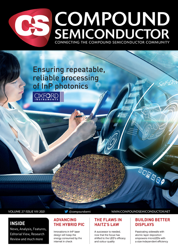
Ensuring repeatable, reliable processing of InP photonics

Advances in the processing of InP lasers and detectors will aid the growth of a third wave of connected devices, following in the footsteps of the computer and smartphone revolutions
BY GRANT BALDWIN AND MARK DINEEN FROM OXFORD INSTRUMENTS PLASMA TECHNOLOGY
Just before the dawn of the 21st century, when many feared a digital Armageddon from the Millennium Bug, a new expression entered our vocabulary: the smartphone. Back then, owners of mobile phones were benefitting from incremental advances in capability that started in the 1980s, giving them a device that no longer performed a narrow function, but provided voice and text communication – and possibly some very basic gaming. However, at that time few, if any, would have anticipated the revolutionary advances in the smartphone over the next two decades, propelling it to the generation-defining connected device that changed forever how we exist and interact.
The latest generations of smartphones make it easier for us to perform known functions, while offering limitless and inconceivable functionality. Now we can pay, play, consume, create, share, locate, navigate, communicate and monitor our internal and external environment – at one stage all these functions were unimagined and unimaginable.
For good reason, some believe that the dawn is breaking for another consumer device to deliver a similar explosion in capability and bring an equally epochal change. Up until now automobiles have only really got better and more efficient at performing a narrow, but important function of transporting us from A to B. We are now on the cusp of a profound change, with the automobiles of the not-too-distant future providing a data centre and infotainment hub on wheels that takes you to places. With the inexorable progression toward vehicles that drive themselves and entertain us along the way, due to this additional functionality, the hourly data generated by the automobile is projected to grow exponentially.

Figure 1. InP structures.
According to Statistica, today a moving ‘connected’ car produces 25 GB of data per hour. Storage system developer Tuxera forecast that this will mushroom to between 1 TB and 19 TB per hour for self-driving vehicles. 5G and the ‘cloud’ will be critical to processing and storing this deluge of data, says market analyst Gartner.
But what is the critical enabling technology for 5G and the cloud? Fortunately, fibre-optic networks based on high-performance InP devices are on hand to enable this next wave of connected consumer device. However, given the drastic rise in data being produced, there is a need for considerable investment in infrastructure to move, process and store this new data.
Increasing network capacity is not trivial. For example, there are several challenges associated with reliable, repeatable high-volume production of the high performance InP devices, that play a critical role in the network.
At Oxford Instruments Plasma Technology we are helping engineers to take on these challenges by sharing our extensive process knowledge, while providing cutting-edge systems to chipmakers. These solutions are playing a crucial role in enabling InP to be the catalyst for change.
InP and optical, a perfect match?
The InP-based photonic-integrated circuits deployed in big data centre transceivers and 5G networks are ideal for supporting the required network infrastructure transformation. The natural spectral range of InP, which spans the 1300 nm to 1650 nm domain, is a perfect match for the low-absorption windows of fibre-optic communication. However, to ensure more cost-effective, higher-yield, higher-performance devices, chipmakers must employ robust, innovative InP plasma-processing solutions. Taking this approach will support a scaling-up of manufacturing and help to deliver the desired network transformation.
At the heart of every optical network are a number of transceivers, formed from InP lasers and diodes. The majority of these high-volume optical devices incorporate InP distributed-feedback lasers (DFBs). They are directly modulated, and provide a narrow line width and a high spectral purity. However, due to growing demand for 400 Gbit/s big data centre transceivers, and 25 Gbit/s fronthaul 5G transceivers, industry is rapidly shifting towards external modulation of the laser as this increases transmission bit rates while ensuring much lower chirp. These advances are happening through an increase in the deployment of 1300 nm sources that pair a DFB laser with an electro-absorption modulator, alongside far higher shipments of 1550 nm components that combine a tuneable laser with a Mach-Zehnder modulator.

Figure 2. Oxford Instruments’ Cobra etch system.
To ensure the desired electronic performance, these devices are manufactured using complex multi-step epitaxial deposition, masking and plasma-etch processes. Plasma etch is also employed to create the physical geometric structures – that is, the gratings and waveguides – that modulate and control laser emission. To help engineers master these steps, we offer a market-leading range of InP process solutions, from slow etch for fine features, such as gratings, to solutions for etching ultra-smooth structures (see Figure 1).
Perfecting the processing
Gratings are created by patterning the InP epiwafer with either a photoresist or a silicon dioxide/nitride ‘hard’ mask, prior to plasma etching. The depth and geometry of the finished structures dictates performance characteristics, such as the coupling coefficient, side-mode suppression ratio and the threshold current.
We recommend our Cobra etch system for forming the high-precision gratings in InP. Using a mixture of CH4 and H2, etch rates of 10-40 nm/min are achievable, to form high-quality structures with depths up to 100 nm. With this approach, the two-dimensional mask pattern is accurately transferred through to the InP substrate. Etching creates three-dimensional structures, because the process demonstrates high preference toward removing unmasked InP material while retaining the mask – this is a condition known as high selectivity. With the etch complete, the mask is plasma-stripped to reveal the finished high-precision gratings. In contrast to hot InP plasma etching, we recommend ambient process temperatures, to prevent the photoresist mask from being rapidly consumed mid-process. If this were to happen, it would change the shape of the finished structures and ultimately compromise device performance.
When producing devices that deliver maximum power-to-light conversion relative to light scattering, absorption and noise, there is a need to not only optimise the depth and geometry, but to also realise straight (sloped or vertical), clean and smooth sidewalls. When seeking to achieve higher performance and a deeper etch, there are limits to what can be accomplished with the CH4/H2 chemistry used in the lower-cost ambient temperature process. Essentially, forming structures in the process chamber involves removing exposed InP material with an etch, while simultaneously protecting the newly formed sidewall under the mask by means of passivation. A CH4/H2 etch/passivation chemistry creates a polymer-type sidewall passivation, and while this option has many benefits, it is not the optimum choice for ultra-clean smooth sidewalls.
To overcome this issue, we have developed advanced hot InP plasma processing capability. This technique requires the use of a ‘hard’ mask, because it withstands process temperatures in excess of 150 °C, a regime where photoresist masks will not survive. By using silicon dioxide/nitride hard masks, we open up the process window and allow the introduction of alternative etch chemistries, such as chlorine/argon.
There is great benefit in using chlorine as the etch component. It reacts readily with InP, because chlorine plasma reacts with InP to create InClx. As InClx has a low volatility at ambient temperature, deposition occurs rather than etching, which is undesirable. However, if the process is too hot and the volatility too high, the etch will undercut the mask and compromise the accuracy of the structure.
The key to running at higher temperatures with hard masks is to tune the process temperature to the sweet spot where InClx has sufficient volatility. Once this is achieved, chlorine provides an excellent option as the etch gas. By adopting a non-polymer chlorine/argon process, this approach creates ultra-clean structures (see Figure 3), and highly repeatable results. What’s more, by eradicating polymers from the chamber, there is an increase in the mean-time between cleans and a dramatic reduction to machine downtime.

Figure 3. Ultra-clean structure processed on Cobra etch system.
Controlling the outcomes
To optimise feature sidewall angle and smoothness, process engineers must carefully balance several process parameters, including the gas ratio, run pressure and plasma power. The equipment must also deliver excellent wafer-stage temperature uniformity, as this is critical to maintaining an even cross-wafer volatility threshold. Process engineering is not the dominant driver for controlling sidewall angle and smoothness, because the final outcome is influenced significantly by the mask angle and quality. Consequently, it is critical to use a highly accurate mask opening process.
As well as controlling dimensions and characteristics of the finished structure, there are two more factors that device manufacturers must consider: wafer-to-wafer repeatability and substrate transfer reliability. With our processing systems these requirements are met. According to reports provided by our sizable customer base – we have systems installed in seven of the top ten optoelectronics device manufacturers – once the process is dialled in, wafer-to-wafer repeatability is excellent; and if the incoming mask remains regular and defect-free, finished InP structures are highly accurate and repeatable. While InP is resilient to high temperatures, low pressures and high plasma powers, anyone who has ever handled these wafers will know that they are incredibly brittle. To minimise losses due to broken wafers, we provide a robotic wafer-handling system that is supremely capable of processing high-value InP substrates. This system is adept at transferring the delicate substrates from cassette to chamber and back, and provides some of the lowest loss rates in industry.
A final consideration when using a plasma etch to create structures in InP is when to stop the process. With depth being so critical to device performance, getting this just right is paramount. To ensure this is the case, our Cobra etcher can be fully integrated with endpoint detection and automated process stop capability. Using optical emission spectroscopy, this system can capture and analyse the wavelengths of light emitted by the volatile compounds released during etching. With this insight, it is possible to evaluate structure-depth part way through the process and accurately stop on layers as thin as 10 nm. Post-etch metrology on a 3-inch InP wafer reveals cross-wafer depth uniformity of just ±3 percent (see Figure 4, which shows the endpoint at which the process was automatically stopped).

Figure 4. Oxford Instruments OES automatic process stop capability.
Compound interest?
The breath-taking revolution in handsets over the last few decades has set a compelling precedent for vehicle integrated technology. Automobiles are blessed with fewer limitations associated with form factor and power management, so the functionality potential is astonishing. Fast-forward a few years and drivers could enjoy the likes of: gesture recognition, thanks to GaAs VCSELs; electric-vehicle fast-charge and power management provided by GaN power transistors; and, of course, data transmission, underpinned by InP-based transceivers. These are just a few examples of a connected vehicle ecosystem packed with compound semiconductor technology.
At Oxford Instruments Plasma Technology, we have been at the forefront of compound research and production for decades, and are already offering a full range of volume and niche solutions that are critical to enabling the vehicle integrated-technology revolution.


