
Chinese GaN firm Innoscience goes international
Company adds design and sales support facilities in Santa Clara, California, and Leuven, Belgium
Innoscience Technology, a Chinese comapmy making GaN-on-Si power solutions, has announced the official launch of its international operations in the USA and Europe. Headquartered in Suzhou, China, Innoscience is now poised to support customers through the addition of design and sales support facilities in Santa Clara, California, and Leuven, Belgium.
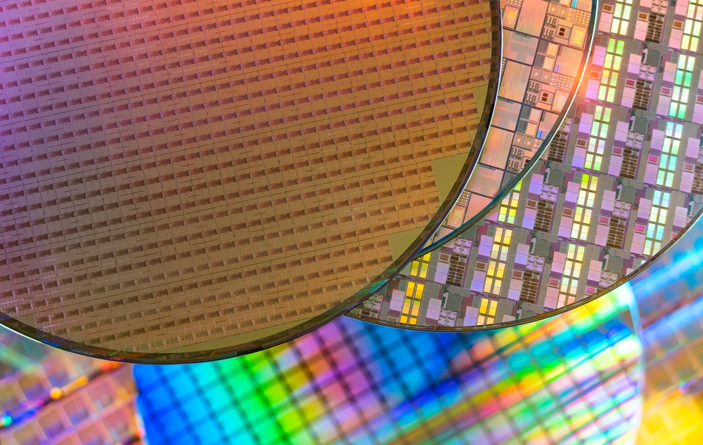
Founded in December 2015, and based in Suzhou, China, Innoscience has two wafer fabs including a large dedicated 8-inch GaN-on-Si site. Currently the company has a capacity of 10,000 8-inch wafers per month which will ramp up to 14,000 8-inch wafers per month later this year and 70,000 8-inch wafers per month by 2025. The company has a portfolio of devices from 30V to 650V and has shipped more than 35 million parts for use in applications including USB PD chargers/adapters, data centers, mobile phones and LED drivers.
Innoscience produces normally-off e-mode GaN FETs. By introducing a stress enhancement layer, the company says it has significantly reduced RDS(on) without affecting other parameters including threshold voltage and leakage. Both epitaxy as well as device processing have been optimized to obtain high reproducibility and yield. Parts have passed quality and reliability tests in excess of JEDEC standards.
Comments Denis Marcon, general manager, Innoscience Europe: "The time is right for GaN, and Innoscience is ready to supply the world. We will surpass anyone on price for an equivalent device and our huge manufacturing capacity means that our customers are assured of security of supply, which is often uppermost in people's minds given the shortage of chips at the moment. We look forward to working with any company in order to proliferate GaN throughout the global electronics industry."
Yi Sun, general manager, Innoscience USA, explained: "This is an exciting time for our customers, who can benefit from Innoscience's applications understanding and demo boards to develop their unique solutions. This will allow us to better support our customers in the USA, and in particular, the Bay area".


