
EVG announces nanoimprint and wafer-level optics system
EVG7300 system targets wafer-level optics, optical sensors and projectors, automotive lighting, waveguides for augmented reality headsets, bio-medical devices, and optoelectronics
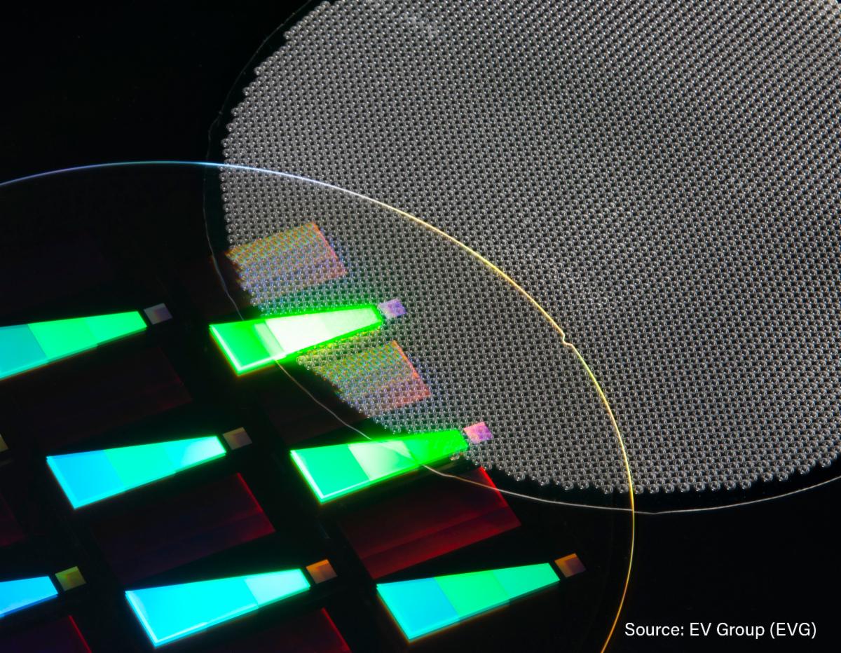
EV Group (EVG), a supplier of wafer bonding and lithography equipment for the MEMS, nanotechnology and semiconductor markets, has introduced the EVG7300 automated SmartNIL nanoimprint and wafer-level optics system.
The EVG7300 is described as the company’s most advanced solution to combine multiple UV-based process capabilities, such as nanoimprint lithography (NIL), lens molding and lens stacking (UV bonding), in a single platform.
The system is designed to serve advanced R&D and production needs for a wide range of emerging applications involving micro- and nano-patterning as well as functional layer stacking. These include wafer-level optics (WLO), optical sensors and projectors, automotive lighting, waveguides for augmented reality headsets, bio-medical devices, meta-lenses and meta-surfaces, and optoelectronics.
Supporting wafer sizes up to 300 mm and featuring high-precision alignment, advanced process control and high throughput, the EVG7300 meets the high-volume manufacturing needs for a variety of freeform and high-precision nano- and micro-optical components and devices.
“With more than 20 years of experience in nanoimprint technology, EV Group continues to pioneer this critical field to develop innovative solutions to meet our customers’ evolving needs,” stated Thomas Glinsner, corporate technology director at EV Group. “The latest introduction to our family of nanoimprint solutions, the EVG7300, combines our SmartNIL full-field imprint technology with lens molding and lens stacking in a state-of-the-art system with the most precise alignment and process parameter control on the market—providing our customers with unprecedented flexibility for their industry research and production needs.”
The EVG7300 system is offered as both a stand-alone tool as well as an integrated module in EVG’s HERCULES NIL fully integrated UV-NIL track solution where additional pre-processing steps, such as cleaning, resist coating and baking or post-processing, can be added to optimize for particular process needs.
SPIE AR/VR/MR Conference
Next week, EVG is giving an invited talk on the benefits of NIL in manufacturing augmented reality waveguides at the SPIE AR/VR/MR Conference and Exhibition, co-located with SPIE Photonics West, which is being held at the Moscone Center in San Francisco on January 22-27.


