
CS International 2021: Laying the foundations for manufacturing microLED displays
Makers of deposition and metrology tools are well prepared to support the launch of high-volume microLED manufacture
BY RICHARD STEVENSON
THE GaN LED is our biggest success story. Launched to market in the 1990s, to date it has enjoyed three ‘killer’ applications: it rose to fame backlighting the keypads and screens of early handsets; it had another rapid increase in revenue from backlighting TVs, tablets and laptops; and it now nets yet more billions by illuminating our homes, our streets and our offices.
Unfortunately, all of these triumphs have come at a cost. The growth of the market has drawn in many new players, driving down margins and commoditising the device. Now there is little interest left in the traditional LED and companies in this sector are looking for new, more profitable opportunities.
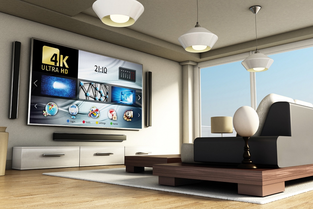
Amongst them, the microLED offers tremendous promise. It can raise the bar for the performance of the display, combining an exceptional contrast ratio with far higher levels of efficiency. Such virtues are valued by the makers of smartwatches, augmented-reality and virtual reality-headsets, TVs and outdoor displays.
But what is needed to unlock this opportunity? Are there tools in place to support such a move? And are we now on the cusp of a revolution in displays?
Offering answers to all of these questions were a handful of speakers at this year’s CS International, held on the 9th and 10th of November at the Sheraton Hotel, Brussels Airport. At this meeting Pars Mukish, Business Unit Manager for Solid-State Lighting and Display at Yole Développement, provided great insight into the state of play of the microLED industry and how it may unfold; and a number of makers of production equipment and metrology tools detailed how they are able to support this nascent industry.
If you don’t have deep enough pockets to shell out $150,000 and pre-order a 110-inch Samsung luxury TV you will argue that the commercialisation of microLEDs is still to take place. But in this very young, dynamic industry it will surely come, given the flurry of patent activity that kick-started in 2014 with the acquisition of LuxVue by Apple. Patent publishing has been climbing at breakneck speed – between 2016 and 2020, this occurred at a compound annual growth rate of 86 percent, according to Mukish. He revealed that display makers are leading the filings, followed by start-ups, with China dominating and South Korea ramping activity in 2020.
Realising cost-effective, high-volume manufacturing of microLED displays will not be easy. Much has been made of the difficulties associated with the mass transfer of millions and millions of red, green and blue LEDs to form the pixels of the displays. But that is by no means the only challenge. There is also the need to make progress on: the cost and the efficiency of the LED; light extraction and beam shaping; generating colours; increasing yield; managing and repairing defects; driver technologies; and establishing a strong supply chain.

Yole Développement is forecasting that the growth in the microLED market will begin with luxury LEDs, before extending to smartwatches, followed consumer TVs, automotive displays and smartphones. Park Mukish presented this figure in his talk: Can microLEDs and laser diodes revolutionise the solid-state lighting industry? Copyright: Yole Développement.
The good news, according to Mukish, is that many potential solutions are being offered for each of these challenges. For example, techniques based on lasers for self-assembly could speed the transfer and assembly of microLEDs to a backplane; and the use of die-shaping techniques, quantum-dot patterning and photonic crystals may be promising pathways for improving the emission from the device.
A substantial reduction in costs is essential to make the microLED a contender for displays. For Samsung’s 146-inch screen that is known as ‘The Wall’ and showcased at CES 2018, the cost associated with the use of 125 µm by 225 µm miniLEDs equated to more than $50,000 per square-metre. To take on a large OLED TV, this figure must plummet by a factor of more than 20, to below $2,000 per square-metre.
By far the biggest opportunity for slashing costs by this magnitude is shrinking the size of the LED. Mukish estimated a cost reduction ranging from a factor of 4 to 70 by diminishing die size. He pointed out that a very significant impact could also come from improving yield and repair, and streamlining transfer and assembly: these two options could trim costs by up to 50 times and 120 times, respectively. Further gains could come from an increase in manufacturing efficiency, which could halve costs.
Mukish offered a route for progress in cutting the cost and size of the LED. There has already been a reduction in the size of miniLEDs on PCB used in Samsung displays showcased at CES, with dimensions down to 35 µm by 60 µm. Alongside this scaling, Samsung introduced a shift in technology to a TFT backplane. This may be used for additional miniaturisation – Mukish speculated its use for 15 µm by 30 µm microLEDs – but to target consumer applications, he sees the need to migrate to die with a vertical architecture, having dimensions of initially 10 µm by 10 µm, followed by smaller sizes.
Upgrading traditional fabs will allow the microLED industry to get off the ground. This will enable the manufacture of microLEDs with dimensions of 10-20 µm that will be deployed in smartwatches, automotive displays and luxury TVs. But for consumer 4K and 8K TVs, which require microLEDs with dimensions no bigger than 10 µm and 5 µm, respectively, new manufacturing approaches could be needed to ensure device efficiency, sufficient yield and device transfer. And further refinements may have to follow for smartphones and augmented reality, requiring devices with dimensions below 3 µm and 2 µm, respectively.
To make displays with microLEDs on such length scales will require dedicated fabs, possibly featuring class 100 air quality, i-line steppers, and tools for ALD, lift-off and wafer-bonding. What’s more, there may be a need for a shift to a semiconductor fab mindset. This would include fab-wide defect and yield management, an increase in in-line metrology and the close monitoring of tools and process excursion.
Mukish warned that progress could be hampered by a lack of standardization. It is risky for equipment makers to develop tools when the task they will be used for has not been defined. And without tools for mass production, it is difficult to set up a supply chain.
Despite this catch-22 scenario, Mukish is forecasting a bright future for displays based on the microLED. By the middle of this decade he expects to see flagship smartwatches on the market that have adopted this technology, and as 2030 approaches, luxury TVs based on microLEDs will fall in price, with this device also starting to appear in automobiles and top-of-the-range smartphones.
Better epi
Echoing the need for a reduction in the size of the microLED, Mark McKee, Director of Product Marketing at Veeco, argued that this must go hand-in-hand with a high yield and the use of large epiwafers – both are critical to reducing cost.
For the making of microLEDs, yield hinges on defect density and wavelength uniformity. For 150 mm and 200 mm substrates, McKee claimed that the defect density must be below 0.1 cm-2. This equates to less than one defect from a transfer field – this is an area of around 15 mm by 15 mm that provides all the microLEDs of a particular colour for one display. According to McKee, for wavelength uniformity the spread across the transfer field must be below 1 nm, and less than 3 nm across the wafer. To meet such specifications, he advocates multi-wafer tools for the growth of arsenide-phosphide LEDs, and single-wafer tools for GaN growth.
Veeco’s leading tool for the growth of arsenide-phosphide LEDs is the Lumina system, which can accommodate seven wafers with a 150 mm diameter. Results on wafers with a peak in photoluminescence at 630 nm show that within the transfer field there is a uniformity yield of around 95 percent. Another encouraging result is finding just three defects on a 150 mm GaAs-based microLED wafer. Results on Veeco’s Propel tool for the high-volume growth of blue-emitting LEDs show that the variation in the photoluminescence peak across a 200 mm wafer is just 1.55 nm.
Hunting for defects
When producing conventional LEDs for demanding applications, fabs can employ end-of-line electroluminescence probing for all devices. With microLEDs this is not an option, so an alternative approach is desired, given the need for minimising imperfections, due to the eye’s sensitivity to any imperfection within a display.
At CS International, Matthew Davies, Head of Industry Applications at Attolight, championed the use of cathodoluminescence for exposing defects in epilayers. This technique, which involves scanning a sample with an electron beam and collecting and recording the emitted light, does not depend on optical absorption and can routinely realise a spot size below 10 nm.
Davies presented the results of a study on epiwafers analysed with the Attolight Säntis 300 platform. This tool is said to provide fully automated quantitative front-end cathodoluminescence metrology and a user-defined recipe interface. In addition, it offers automated data analysis and is capable of cassette-to cassette handling.
In the study presented, Davies and co-workers carried out automated probing of wafers on three length scales. Efforts commenced with fast wafer screening, which detected local variations at the wafer level. A chip-level review followed, uncovering variations between individual chips, before ultra-high resolution imaging exposed intra-chip variations.
To ensure that screening of the whole wafer offers a fast, insightful review, scanning occurs over multiple channels. By applying differential analysis to this data, engineers can identify shifts in peak wavelength, alongside variations in the intensity and width of the signals. This can uncover local ‘hotspots’ on variable length scales, exposed by extremes in the data.
Davies presented results of fast screening on a 100 mm wafer. This provided an easy discrimination of surface and buried particles by comparing the cathodoluminescence image with the scanning electron microscopy image, also provided by the Säntis 300 platform. According to Davies, extremes in data in good regions with a length scale of hundreds of microns are equivalent to extremes of data in regions covering several millimetres, implying that there is no need to probe all of a wafer to obtain reliable data.
The fast scan results allowed Davies and colleagues to select the best, the worse and the median ‘performers’ from a region. Using cathodoluminescence to image these chips with a high resolution unveiled the local threading dislocation density, while the corresponding scanning electron microscopy image offered insights into chip shape, etch deposits and mask transfer uniformity. By comparing the performance of the best, worse and median chips from different regions of the wafer, regional viability maps were constructed. Davies claimed that the identification of low viability regions reduces the feedback time on critical process steps; lowers the total probing costs, by optimising the time spent during a subsequent metrology step; and speeds time to market, by accelerating the time taken to understand which process changes have the biggest impact on viability.
Ultra-high resolution mapping, which Davies sees as an optional extra, employs a pixel size below 100 nm. Imaging at this length scale provides an insight into the local threading dislocation density and allows evaluation of the emission wavelength homogeneity, the intensity homogeneity at the chip level, and the shape and uniformity of the mesa edge.
Tools for vertical LEDs
One of the implications of shrinking the size of the microLED, and the resulting shift from the flip-chip to the vertical architecture, is the need to introduce new tools and processes to some LED fabs. Two of the key features of a vertical LED are an ITO layer that provides a transparent, current spreading layer and a distributed Bragg reflector (DBR) for boosting light extraction – examples of equipment that can add these features formed the focus of a presentation given by Stefan Seifried, Head of the Optoelectronics Business Unit at Evatec.
Seifried explained that Evatec offers tools for single-wafer and batch deposition of ITO, both accomplished with a low-damage process. For a batch process, Evatec offers the CLN 200 BPM, which can handle substrates up to 200 mm in diameter and vary the ITO deposition temperature from below 80 °C to as high as 350 °C. Using this tool, on 150 mm substrates ITO thickness uniformities across the wafer, between wafers and between runs are below 1 percent for 15 nm-thick and 100 nm-thick layers. Switching to 200 nm substrates degrades the uniformity of the ITO thickness, with the greatest level of non-uniformity found within-wafer on 15 nm-thick films – in this case, non-uniformity is 3 percent.
When ITO is deposited on the epilayers, it forms grains with dimensions that vary with process condition. Increasing the temperature and the throw distance leads to increases in grain size.
The CLN 200 BPM can also be employed to deposit a stack of oxide films that form a DBR. Seifried shared results for a 10-layer stack assembled from alternating SiO2 and TiO2 layers. The mirror had a reflection band centred around 570 nm with a reflectivity of 98.4 percent. Uniformities across 150 mm-diameter wafers, between them and between runs are no more than 0.5 percent, when evaluated by considering values for 90 percent reflectivity. Increasing the DBR stack to 29 layers propelled reflectivity to 99.8 percent.
ALD advantages
Another option for depositing thin films, promoted at CS International by Beneq’s Head of Worldwide Sales, Mikko Söderlund, is atomic layer deposition (ALD). Söderlund argued that the attributes of ALD include: its gentle, sequential gas-phase process; the formation of dense, pinhole-free coatings with unrivalled conformality; a process window spanning 70 °C to 400 °C that is well-suited to back-end-of-line processing; easy process control and repeatability; the opportunity to scale by batch processing; and a good selection of materials with tuneable properties.
According to Söderlund, ALD can be used to improve the performance of the microLED. Using this technique to passivate sidewalls, possibly with a film of Al2O3, increases external quantum efficiency while lengthening lifetime, lowering leakage current and minimising wavelength shifts. ALD can also be used to produce DBRs with a thickness precision that is sub-nanometre, and a nanometre thickness uniformity. There is also the possibility to produce coatings with an incredible level of resistance to moisture.
To carry out all these processes, Beneq offers the Transform portfolio. This suite, combining thermal and plasma-enhanced ALD processing modules, enables single-wafer and batch processing. These tools can accommodate wafers up to 200 mm in diameter – 300 mm is on the roadmap – and provide deposition of a wide variety of thin films, including Al2O3, SiO2, HfO2,Ta2O5, TiN, AlN, SiN and ZnO.
These ALD tools, plus those providing other deposition techniques and metrology, are sure to play a key role in the emergence of the microLED industry. Progress over the coming months will be reported at the next CS International, held on 28-29 June 2022, so save the date now so you can follow the latest developments in this very promising sector.


