
Hexagem: the only way is up
With GaN poised for massive market growth, Sweden start-up Hexagem is set to deliver GaN-on-silicon wafers for vertical devices, with a difference.
As industry players far and wide eye GaN devices with increasing excitement, one Sweden-based start-up plans to shake-up the market with its disruptive technology.
Lund University spin-out, Hexagem, is pioneering a vertical nanowire growth process to make GaN-on-silicon semiconductors as efficient as the market's best GaN devices. What's more, the devices are set to contain far fewer defects per square centimetre than today's typical lateral GaN devices, spelling good news for device manufacturers such as Infineon and ST Microelectronics.
As chief executive, Mikael Björk says: “At present, [our semiconductors] have 100 million defects per square centimetre. But we believe that we can significantly improve the material quality and soon approach 10 million defects per square centimetre and thus surpass the competition.”

Mikael Björk, chief executive at Hexagem. [RISE/ David Lagerlöf]
While Hexagem span out from Lund University back in 2015, it's big break came in 2019 when it won just over €2 million in European Union funds to coordinate 'eleGaNt'. Here, the project goal was to develop its newly patented method of growing high quality GaN layers on any substrate.
“The company had been carrying out a lot of university research but this large EU grant meant we could really expand and hire more people.” says Björk.” I joined [shortly afterwards], which was basically the beginning of the pandemic but we've been able to continue work with very few hiccups.”
Key to this has been Hexagem's partnership with RISE Research Institutes of Sweden - a hothouse of GaN activity and home to the ProNano testbed for pilot and large-scale GaN device fabrication. Michael Salter is senior project manager at RISE, and as he puts it: “With ProNano we are building a pilot manufacturing infrastructure to support startup companies, like Hexagem, by demonstrating and accelerating their technology to the market.”

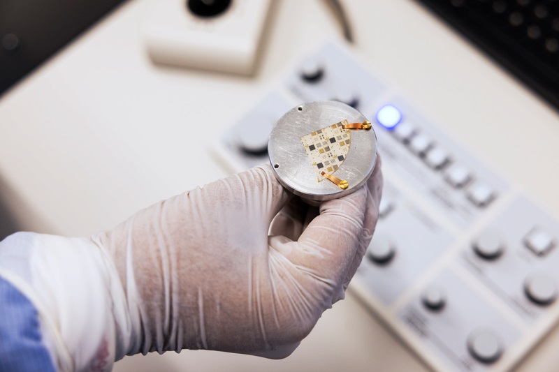
MOCVD at ProNano. [RISE/ David Lagerlöf]
Key facilities include cleanrooms, an Aixtron MOCVD reactor as well as metrology, scanning electron microscopy facilities. Critically, Hexagem has been honing its GaN-on-silicon processes here, using MOCVD to create nanowires that eventually form thin layers of GaN on the silicon wafer.
As part of the process, a silicon nitride buffer layer is deposited onto the silicon wafer, which is then patterned with arrays of holes ready for selective epi-growth of the dislocation-free GaN nanowires. Once the nanowires are grown, sidewall epi-growth then takes place to widen the nanowires until these almost impinge on each other, giving a coalesced GaN layer.
“We're 'reshuffling' the material via epitaxial growth to fill the voids and give us this planar film,” says Björk. “If you do this properly, you get very few dislocations.”
Excitingly, the Hexagem chief executive officer reckons he and colleagues will grow layers as thick as 10 micron on silicon wafers this year, which is sufficient for the fabrication of the high voltage vertical GaN devices that many in industry have been chasing for some time. “We also think we'll be able to use thinner and lower quality buffer layers to grow our wires on top - this will also save costs,” he adds.
GaN with a difference
Vertical GaN devices are not new. Thanks to the promise of extremely efficient devices that can switch at higher frequencies than conventional lateral devices and operate at very high voltages, myriad researchers have been developing vertical GaN semiconductors with a handful of businesses racing to get the technology to market. US-based NexGen Power Systems, for one, is growing low defect-density epi-layers onto bulk GaN substrates.
However, Björk believes that Hexagem's approach is unique. “We are working with silicon substrates in combination with the unique nanowire coalescence - I doubt anyone else is doing this,” he highlights.”
“Of course, we use lithography and patterning that isn't standard in epitaxy but cost-wise we will compensate by using those less thick buffer layers on the silicon,” he says.“This is not a cost-play game for us – it's about quality... and once we get to larger wafer size we could be even cheaper, although this remains to be seen.”
Hexagem has been working with 50 mm wafers but trials on 150 mm wafers are currently underway. According to Björk, the company is also in discussions with several 'big industrial players' on scaling the technology. Indeed, the company has links with Infineon and Bosch through other EU-funded projects, UltimateGaN and YESvGaN.
“Commercial scale today is 150 mm but we also want to go for 200 mm wafers,” says Björk. “It's still a couple of years away but we're really pushing for the current 150 mm demonstration right now... Thanks to our unique strain compensation methods we think we can enable at least 10 micron thick layers on these larger wafer sizes, and this could take us to 1200V vertical devices.”
Looking forward, Björk says Hexagem has no plans to build production facilities but intends to licence its technology to industry heavyweights. He expects power electronics markets, including electric vehicles, will be the first stop for his GaN-on-silicon wafers but is also interested in fabricating materials for RF and optoelectronics applications. And ever-thicker layers are also on the horizon.
“We'll keep on improving quality and enabling thicker layers,”he says. “We can use our technology to also grown on SiC and sapphire wafers but there could opportunities to transfer layers to, say, a metal contact or other substrates – there are a lot of interesting things to look at.”


