
Taking GaN CMOS to the IC
Forming logic circuits with a power HEMT platform that features a p-GaN gate provides a significant step towards unlocking the full potential of GaN integration
BY ZHEYANG ZHENG, LI ZHANG AND KEVIN CHEN FROM THE HONG KONG UNIVERSITY OF SCIENCE AND TECHNOLOGY
CMOS technology continues to prevail in very large-scale and mixed-signal ICs. In these forms of circuit, CMOS has dominated for the past four decades, thanks to topping the list of the most energy-efficient circuit topologies. Whenever new electronic devices are explored in other semiconductor materials, there is a hunt for complementary devices, to see whether this could lead to a superior successor to silicon CMOS. However, such a pursuit tends to be full of obstacles, with GaN providing a typical example.
This wide-bandgap semiconductor, blessed with an inherent capability to form a very high-mobility two-dimensional electron gas (2DEG) channel, has many attractive attributes. This has driven widespread deployment of n-channel GaN HEMTs in 5G base stations, as well as ultra-compact power adaptors and supplies for mobile devices. In the near-term, more exciting applications are sure to emerge that are power-hungry, yet demand ultra-compactness in power supplies. This will create an appreciable market for GaN. However, much is still to be done when it comes to GaN CMOS. Efforts have been held back by undesirable material properties for implementing p-channel FETs and a lack of essential applications that would spur development.
Part of the problem with p-channel devices is the very low hole mobility in GaN. It is typically just 20 cm2 V-1 s-1, compared with around 2000 cm2 V-1 s-1 for the electron mobility in the 2DEG channel. Such a low value dampens the interest of many researchers. What’s more, there doesn’t appear to be a need for GaN CMOS in power amplifiers and power switches. GaN HEMTs tend to act as powerful discrete devices, usually incorporating a very large gate width for regulating high currents and handling high powers. Consequently, despite the rapid development of GaN HEMTs, demonstrations of GaNp-FETs are few and far between, with efforts related to CMOS logic inverters even rarer.
Now the situation has started to change. With GaN power HEMTs intensively advanced, peripheral circuitry is starting to become a non-negligible performance-limiting factor for the entire power conversion system. Parasitic inductances are the most undesirable but inevitable issue – they are induced by interconnections between power HEMTs and other off-chip functional blocks, such as the gate driver and miscellaneous sensing modules. By hampering the continuous push towards higher operating frequencies, these inductances are compromising the superiority of the GaN HEMT. One promising solution is monolithic integration – that is, the deployment of as many peripherals as possible on the same chip as the GaN HEMTs.
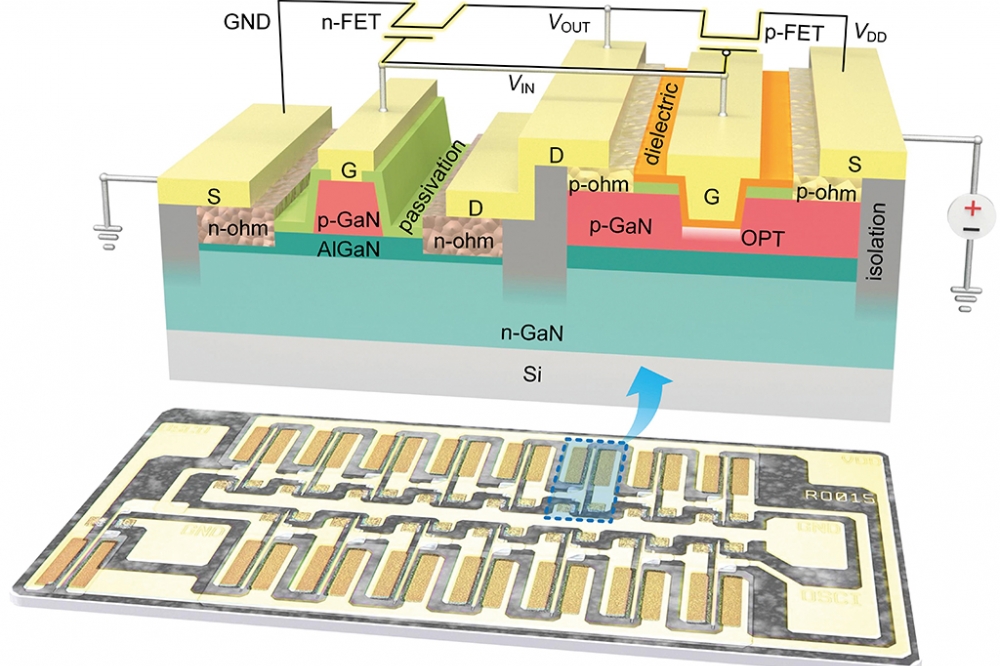
Our team at The Hong Kong University of Science and Technology (HKUST) have been developing integrated GaN technology for many years. The planar structure for this class of device inherently favours high-density monolithic integration (see Figure 1).
Back in 2009 we proposed the concept of ‘GaN smart power systems’, and since then we have kept on advancing this technique, working in partnership with colleagues in academia and industry.
As more and more functional blocks have been demonstrated, and entire systems have got more and more complicated, there has been a significant increase in the use of logic circuits. In fact, it is these logic circuits that make the power system ‘smarter’ and more intelligent. For GaN, logic circuits are still constructed from just n-channel FETs. Due to this, as the number of logic gates increases, power consumption has become a concern. It is this state-of-affairs that hampered the silicon-based ICs of the late 1970s. Back then, NMOS logic circuits consumed too much power, giving rise to CMOS.
With a potential beneficiary in mind, we wanted to develop GaN CMOS. Due to the low mobility of holes, we knew that this technology would never be deployed in cutting-edge ultra-high-speed/low-power logic ICs. However, it could deliver on-chip logic services for specific applications, such as power electronics, thanks to its high energy efficiency. We were also intrigued in how much we could benefit from the p-GaN epi-layer that is readily available in the p-GaN gate power HEMT technology, a dominant platform for commercial GaN power electronics.
The GaN CMOS family
Three immediate benefits come from using the commercial p-GaN gate HEMT epi-structure to produce GaN CMOS ICs. First, this enables straightforward integration with the power HEMT. This is most welcome, given the commercial opportunity associated with the monolithic integration of high-energy-efficiency peripheral logic gates with power switches. Second, owing to the maturity of power HEMT technology on this platform, GaNn-FETs for CMOS ICs are naturally ready. All that’s required to move from power to CMOS is to make some simple changes in the physical layout, because n-FETs for both applications share exactly the same device structure and fabrication steps. Third, the p-GaN layer is designed to deplete the 2DEG channel underneath, which could only be restored by removing the p-GaN layer above. This enables the p-channel and n-channel to be naturally de-coupled, suppressing crosstalk.
Drawing on the commercial p-GaN gate HEMT platform, our team has fabricated a large set of elementary CMOS logic gates. They include the inverter, which clearly shows almost all desired ‘CMOS properties’, such as: rail-to-rail output; adaptively varied transition thresholds, roughly following half of the supply voltage (VDD); substantially suppressed static power; a very high voltage gain; and broad noise margins. More importantly, thanks to the use of a wide bandgap material, our CMOS logic inverter demonstrates satisfactory thermal stability (see Figure 2). When considering static characteristics, the presented GaN CMOS inverter is almost perfect for use.
We have also demonstrated a NAND gate, a NOR gate, and a transmission gate. All three exhibit rail-to-rail outputs and deliver correct functions at megahertz-level frequencies (see Figure 3). By demonstrating this logic gate family, we have shown that, in theory, the essential building blocks of any logic function can be readily designed and implemented. From this foundation we have gone on to show that by cascading these blocks in certain ways to form more complex logic circuits, it is possible to construct multi-stage logic circuits, such as a monolithic 15-stage ring oscillator oscillating at a sub-megahertz frequency (see Figure 4).
Realising E-mode p-FETs
The key to realising GaN CMOS ICs is to produce satisfactory GaNp-FETs on the selected platform. With our commercial p-GaN gate HEMT epi-structure, we enjoy appreciable benefits, but they come with stringent restrictions. For example, to ensure a sufficiently E-mode operation of the power HEMT, the p-GaN must be heavily doped and sufficiently thick to prevent punch-through at a high gate bias.
It is essential to include a recess in the design. Otherwise, the p-GaN, which is thick and heavily doped, could never be depleted by the gate, as the electric field would become dramatically high and induce a catastrophic breakdown. Once only a moderate portion of p-GaN is removed – for example, by still retaining 30 nm of p-GaN – the channel can be turned off with a positive gate voltage. Operating in this manner, the p-FET works in a depletion mode.
However, a more significant modification to the design is needed to form E-mode FETs, which are mandatory for realizing ICs with truly ‘CMOS-like’ behaviour (especially, completely suppressed power dissipation at static states). One option is further thinning of the channel. However, while this drives the device into E-mode, this comes at the expense of a significantly reduced on-state current, because the channel for current conduction is too thin. Of greater concern, though, is the poor-quality of the etched p-GaN surface that introduces strong scattering to holes in the very thin p-channel.
By adopting a novel approach to solve this dilemma, we have maintained a reasonable on-state current density while realizing E-mode operation. This is accomplished with an architecture that combines a moderate recess with an oxygen plasma treatment to the recessed p-GaN surface. With this approach, we realise E-mode operation in a ‘gentler’ way (see Figure 5 for a comparison between our device and the conventional alternative). We use an oxygen plasma treatment to convert the top layer of retained p-GaN free-of-holes, thereby facilitating depletion of the p-channel buried below. It is possible that oxygen appearing in the p-GaN could act as a shallow donor, ionising electrons to recombine with holes; or it could form Mg-O complexes, passivating the magnesium acceptor directly (see Figure 6).
Operating with a negative gate bias, the holes in our E-mode FETs can be restored to the buried p-channel. This maintains a high hole mobility, because it is separated from the plasma-etched problematic interface between the oxide and p-GaN by the region treated by the oxygen plasma. Thanks to this, the buried-channel GaNp-FET exhibits decent electrical characteristics. The threshold voltage is stringently negative, and the on-state current density reasonable, exceeding 6 mA/mm. Overall, the on/off-state current ratio can reach seven orders of magnitude. We believe that the well-suppressed off-state leakage current could be attributed to a combination of: an insulating gate structure that guarantees a very low gate leakage; a stringent E-mode operation, which ensures a fully depleted channel; and a fluorine ion-based planar isolation technique that eradicates detrimental leaky sidewalls.
While there is still much room for further optimization, the performance delivered by this commercial platform-based p-FET is already impressive, and shows that developing CMOS ICs on exactly this platform is highly feasible. Building on this start, we had the motivation to construct CMOS ICs, and produce the first GaN CMOS IC family.
Performance projections
There are two aspects to evaluating the potential and the utility of GaN CMOS. One is the limit of its operating speed, given restrictions related to material properties and fabrication capabilities, and the other is the extent of energy savings associated with replacing n-FET-based logics with CMOS logics.
Right now it is not that practical to build circuit models for simulation-based studies, because the currently available devices have not been intensively optimized. So to gauge the potential of GaN CMOS, we have conducted an analysis using reasonable simplifications. This revealed that the operating speed of GaN CMOS will comfortably satisfy the requirement of GaN-based power systems and, as expected, that GaN CMOS is capable of significantly reducing power loss in the interested frequency regime.
A sufficient operating speed may come as a surprise, given the massive mismatch between the mobilities of electrons and holes that leads to a two-orders-of-magnitude difference in the current density of n-FETs and p-FETs (see Figure 7 (a)). Due to this, GaN CMOS logic gates inevitably exhibit asymmetric rising and falling edges. However, it is the average delay time that determines the speed of the circuit.
At the circuit level, what matters is to optimise the device ratio between the p-FET and the n-FET. When there is a hole mobility of 20 cm2 V-1 s-1, using a gate length of 0.5 mm enables an optimum delay time that’s less than 50 ps (see Figure 7 (b)) – that is sufficiently fast.
When judged in terms of energy efficiency, there is no doubt that CMOS outperforms n-FET-based logics, such as DCFL, which is short for direct-coupled FET logic (see Figure 8). In CMOS circuits static power dissipation is negligible, with power loss mainly coming from the shoot-through current and a charging and discharging of the capacitor during transition states. But for DCFL circuits, static power dissipation dominates. Note also that as the operating frequency increases, so does the power dissipation of GaN CMOS. However, despite these concerns, in the interested frequency regime of a power system – it has a typical operating frequency ranging from 100 kHz to 10 MHz – CMOS has the potential to dramatically reduce power loss.
Toward real applications
Based on constraints associated with material properties and fabrication, we believe that GaN CMOS will deliver a promising performance when used for power integration. To facilitate an actual application, in addition to the need for substantial downscaling and process optimization that would boost up the current density of p-FETs, there is another critical issue: examining and improving stability at the device and circuit levels. On this mature platform it will come as no surprise that the stability and reliability of the n-FET has been substantially studied and enhanced. So what’s needed is to focus on the p-FET.
One option for mitigating the strong scattering within the p-FET is to use oxygen plasma treatment to separate the conducting channel from the troublesome etched interface. However, the downside is a sub-standard quality for the etched interface. Due to this weakness, when a large gate bias is applied, holes traversing the device get trapped at the interface, leading to a variation in the threshold voltage.
We tackle this problem with a two-step strategy. Our first move is to replace the Al2O3 gate dielectric with SiNx. As the latter aligns with GaN in a type-II manner, it presents no barrier to holes in GaN. According to the disorder-induced-gap-states model, which can generally describe the interface between GaN and oxides, there is an appreciable trap density near the band edge of the former structure. Our switch to SiNx introduces a hole evacuator, automatically nullifying the high-density hole traps near the valence band edge. The upshot is the prevention of successive shifts in threshold voltage at highly negative gate biases (see Figure 9 (a) and (b)).
However, this in itself is not a great solution, as there is still notable hysteresis, attributed to deeper trap states that align with the bandgap of SiNx and are thus not easy to evacuate. To tackle this issue, we take a second step in gate stack engineering, converting the region that we have treated with an oxygen plasma into crystalline nano-phase, gallium oxynitride (GaON). Previously, we used GaON to improve the gate reliability of a p-GaN gate HEMT. Through that effort, we learnt that GaON possesses a much better thermodynamic stability and a higher material quality than GaN subjected to an oxygen plasma treatment. Introducing GaON has had a profound effect, completely eliminating hysteresis (see Figure 9 (c)).
Our staggered gate stack differs from the conventional metal-insulator-semiconductor stack. In our case, the dielectric does not provide a barrier for blocking carriers when the device is in its on-state. Due to this, we need to include a buried-channel structure. When operating in the on-state, the holes in the channel are confined by the built-in potential in p-GaN, enabling the gate leakage to remain at a very low level if the gate bias does not exceed - 6 V. Yet, the SiNx is indispensable. It effectively blocks the gate leakage at the off-state under a positive gate bias; and it serves as a voltage divider, expanding the allowed input swing to fit the p-GaN gate HEMT platform, where typically 5-6 V are usually used to drive n-FETs.
By turning to our SiNx/GaON gate structure, we are able to extend the operating temperature of GaN CMOS ICs to 400 °C (see Figure 10). With a 5 V voltage supply, the logic transition threshold fluctuates within only 0.4 V. At this supply voltage, the rail-to-rail output swing is well maintained, degrading only slightly at 400 °C, due to an increase in leakage that could be further suppressed with process optimization. These results underscore the superiority of GaN as a wide-bandgap semiconductor, indicating possible applications of GaN in extreme environments.
We have made major strides with GaN CMOS, demonstrating the first family of ICs and also projecting performance in power integration and substantially improving stability. Our next steps, hopefully taken in collaboration with industry partners, are to undertake device downscaling, silicon-compatible process development and yield/uniformity improvement. There is no doubt that GaN CMOS is marching toward practical applications.
Captions
A 15-stage GaN CMOS ring oscillator and a schematic of a typical GaN CMOS inverter.
Figure 1. One attractive approach to fully unlocking the potential of GaN in power electronics is the monolithic integration of the entire power conversion system. (a) depicts a GaN-based smart power platform. (b) illustrates that when a logic inverter is made of n-FET-based topologies, such as directly-coupled-FET-logic (DCFL), there would be one logic state when the gate has significant static power dissipation. Using the CMOS topology instead could guarantee the suppression of static power dissipation at both states; (c) is a cross-section view of available components on the p-GaN gate power HEMT platform. The on-chip CMOS logics would be inducted onto this platform.
Figure 2. A GaN CMOS logic inverter shows impressive quasi-static performances, including rail-to-rail operation, VDD-adaptive and well-placed transition thresholds, substantially suppressed static power dissipation, broad noise margins, and high thermal stability.
Figure 3. HKUST has demonstrated a full family of elementary logic gates with GaN CMOS. This figure shows their photos, circuit diagrams, and operating waveforms with sub-megahertz frequencies.
Figure 4. Demonstration of multistage GaN CMOS logic ICs. The team at HKUST uses a 15-stage ring oscillator composed of GaN CMOS logic inverters as an example, showing its oscillating waveform and power spectrum.
Figure 5. Approaches to realising E-mode p-FETs on the p-GaN gate HEMT platform. One option is to gradually thin down the gated region to drive the device from always-on to D-mode and then E-mode. However, the aggressive etching would significantly reduce the on-state current. The team at HKUST has taken a different approach, adopting a ‘moderate gate recess + oxygen plasma treatment (OPT)’ to realize E-mode operation while maintaining reasonable on-current.
Figure 6. Working principle and device performance of a buried channel GaNp-FET formed using an oxygen plasma treatment. (a) shows energy band diagrams of the off-state (with VGS = 0 V) and the on-state (with VGS< VTH); (b) and (c) conceptually show possible mechanisms of why oxygen plasma treatment could convert the p-GaN surfaces to free-of-holes. (b) shows that oxygen acts a donor to ionize electrons to compensate holes. (c) shows that oxygen forms a Mg-O complex to directly passivate the acceptor. (d) and (e) plot transfer and output characteristics of the p-FET, respectively. The p-FET exhibits stringent E-mode operation, reasonable on-state current density, and a high on-off ratio.
Figure 7. The performance of the n-FET and p-FET on the p-GaN gate platform determine the optimization of the propagation delay at the circuit level. (a) Given the significant mobility mismatch between electrons and holes, the n-FET and p-FET exhibit a two-orders-of-magnitude difference in current density. (b) With device ratio, b, increasing, the average propagation delay firstly drops and then rises. Thus, there is an optimum value of b, which is around the inverse of the square root of the mobility ratio. (c) Reducing the gate length could reduce the delay in a quadratic way. Overall, it is achievable to realize a sub-nanosecond delay for GaN CMOS logic gates, which could satisfy the requirement of current GaN-based power conversion systems.
Figure 8. By replacing the DCFL logic circuits with CMOS logic circuits, the power loss induced by logic blocks would be greatly reduced, because the static power dissipation (Pstc) in CMOS circuits is negligible. (a) shows that for a CMOS logic gate, dominating power dissipation components are contributed by the shoot-through current (Psh-th) and the capacitance charging/discharging current (Pcap). Both arise at transition states and thus the total power dissipation (Ptot) increases with frequency. (b) shows that for a DCFL logic gate, the dominating component is Pstc (in this case Psh-th is included in Pstc). (c) shows that when the switching frequency is lower than 100 MHz, CMOS circuits have significantly lower power loss than DCFL circuits.
Figure 9. The unoptimized gate stack results in pronounced hysteresis loops in dual-sweep transfer curves. Such an instability in the threshold voltage (VTH) is very likely induced by the problematic dielectric/p-GaN interface. Utilizing the buried-channel structure of this p-FET, the team at HKUST replaced Al2O3 with SiNx, which exhibits no hole barrier to GaN, and found that the VTH shift induced by highly negative VGS has been effectively suppressed. The VTH shift induced by a small VGS is eventually suppressed by converting the OPT-treated p-GaN surface to GaON, which eliminates high-density interface traps.
Figure 10. With the stability of p-FETs greatly enhanced, the GaN CMOS logic inverter exhibits remarkable thermal stability up to 400 °C. The transition threshold only varies slightly, whereas the rail-to-rail output is well preserved until the temperature reaches 400 °C to induce notable leakage. These results show that GaN CMOS is very promising for use in harsh environments.


