
Refining the quantum dot laser
Increasing the density of dots by at least an order of magnitude promises faster lasers with a lower threshold current
A team from Japan claims to have broken new ground by cranking up the density of quantum dots in lasers that could serve in optical networks and biomedical measurement systems.
By increasing the density of dots by at least an order of magnitude, the engineers at The University of Electro-Communications in Tokyo have slashed the number of active layers in the device. According to team spokesman Koichi Yamaguchi, while conventional quantum-dot lasers have around ten active layers, their devices can have just one or two of them.
Yamaguchi revealed that one of the merits of trimming the thickness of the active region is enhanced carrier recombination.
“In addition, the in-plane ultra-high-density quantum-dot layer is expected to not only reduce the threshold current, but increase the carrier incorporation rate into the quantum-dots and enhance high-speed modulation.”
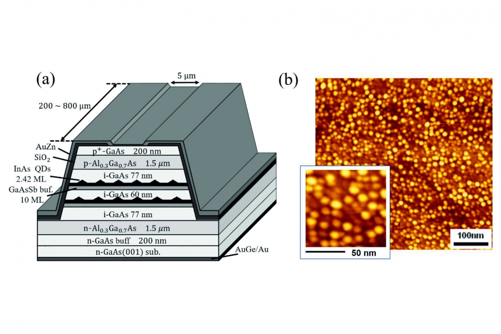
Fabrication of the team’s lasers began by loading an n+ GaAs (001) substrate into an MBE reactor and depositing an epitaxial stack consisting of a 200 nm-thick n-type GaAs buffer layer, a 1.5µm-thick n-type Al0.3Ga0.7As bottom cladding layer and a 220 nm-thick undoped GaAs-based waveguide. The latter features a pair of layers containing an ultra-high density of in-plane InAs quantum dots, deposited at 470 °C and formed on a GaAsSb buffer layer using the Stranski-Krastanov growth mode.
The picture above shows how the ridge waveguide lasers have just two quantum dot layers (a), thanks to the high density of dots, seen in atomic force microscopy images (b).
X-ray diffraction measurements of this heterostructure indicated that the antinomy content in the buffer is between 12 and 14 percent. According to atomic force microscopy, the density of the dots is 5 x 1011 cm-2. The team attributes an antinomy surfactant effect to suppressed coalescence of the dots, which are typically 1.4 nm high and 14 nm wide.
To complete the fabrication of the lasers, the engineers added a 1.5µm-thick p-type Al0.3Ga0.7As top cladding layer and a 200 nm-thick p+ GaAs contact layer. Subsequent photolithography and wet-etching created a 20µm-wide ridge-waveguide structure. Magnetron sputtering of a 200 nm-thick SiO2 film followed, prior to defining 5µm-wide or 7µm-wide windows and then adding a pair of electrodes – one to the substrate and another to the p+ GaAs contact layer. Finally, the team cleaved the patterned substrate into laser chips to create cavity lengths ranging from 200µm to 800µm.
These lasers, which could deliver an even better performance by forming high-reflectivity coatings on their facets, have a threshold current density of 1-10 kA cm-2. While continuous-wave lasing at room-temperature occurs at just 1021 nm, emission could be shifted to the 1.2µm to 1.3µm range by adding a GaAsSb capping layer.
The researchers claim that when their lasers operate at room temperature, there is a strong coupling of the wavefunction between neighbouring quantum dots. This gives rise to a miniband in the conduction band that results in a characteristic temperature that the team describes as “not so high”.
Based on an analysis of the dependence of the cavity length on threshold current density, Yamaguchi and co-workers have concluded that their devices have a comparable crystal quality to other quantum-dot lasers. What’s more, they have said that by increasing the length and reflectivity of the cavity, their lasers realise a lower threshold current density.
By comparing the threshold current of the team’s laser with another design, the researchers estimate that just 41 percent of the dots in the latest design contributed to lasing. They attribute this weakness to inhomogeneous broadening.
“The uniformity of the in-plane ultra-high-density quantum dots is still insufficient,” argued Yamaguchi. “So, it is necessary to promote high uniformity in future.”
REF
M. Tanaka et al. Appl. Phys. Express 14 124002 (2021)


