
Realising a high UV efficiency on sapphire
AlN templates with a face-to-face anneal enhance deep-UV LED efficiency
The internal quantum efficiency of active regions that emit in the deep-UV can now be almost as high on AlN templates as they are on native bulk substrates, claims a team from Japan.
By minimising light-quenching dislocations with a templates formed with sputtering and annealing, the team – a partnership between Yamaguchi University, the National Institute of Technology and Mie University – has fabricated multi-quantum-well heterostructures with an internal quantum efficiency of 90 percent.
Spokesman for these researchers, Yoichi Yamada from Yamaguchi University, told Compound Semiconductor that the collaboration expected a very high quantum efficiency from its samples because calculations predicted a value of more than 80 percent for a dislocation density of 2 x 108 cm-2. “Our study has shown that [efficiency] experimentally for the first time.”
This success could underpin an increase in the bang-per-buck of commercial deep-UV LEDs. Those built on a bulk AlN foundation have an excellent internal quantum efficiency, but are high in cost, due to the expense of the substrate.
As well as cutting costs, using a sapphire substrates for this class of emitter aids process development and improves reliability, as demonstrated by the progress of the blue-emitting LED.
“In addition, the refractive index of sapphire is close to that of silicon dioxide, making it advantageous in light-extraction structures”, remarked Yamada.
He and his co-workers have fabricated light-emitting active regions on templates that are formed by sputter-depositing AlN films on c-plane sapphire substrates, which are off-cut by 0.2 ° toward the m-axis. To improve material quality prior to MOCVD growth, the researchers put faces of pairs of AlN templates together before annealing them under nitrogen, typically for several hours. According to X-ray diffraction measurements, this process reduced the screw and edge components of dislocations in the AlN film to just 1.2 x 106 cm-2 and 3.3 x 108 cm-2, respectively.
On this foundation the team added an active region, formed from ten Al0.50Ga0.50N quantum wells with a thickness of 2 nm, separated by 6 nm-thick Al0.75Ga0.25N barriers. Doping the wells and barriers with silicon decreased the density of non-radiative recombination centres consisting of cation vacancies. To provide a benchmark for evaluating that light-emitting structure, the team replicated the active region on an MOCVD-grown AlN template that had screw and edge dislocation densities of 2.9 x 107 cm-2 and 9.1 x 108 cm-2, respectively.
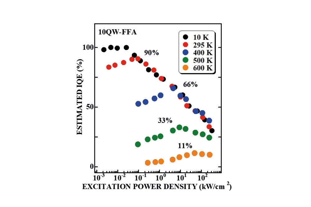
Internal quantum efficiencies were deduced by making photoluminescence measurements at various temperatures, and assuming that this efficiency is 100 percent at absolute zero. This methodology determined a value of 90 percent for the room-temperature internal quantum efficiency of the sample with a foundation formed by sputtering, compared with just 58 percent for the control.
By considering the internal quantum efficiency at a range of excitation densities, the team uncovered an efficiency plateau at 10 K in the sample containing a sputtered template. This feature revealed that at low excitation densities, non-radiative recombination centres are either fully saturated or completely frozen. In comparison, at that same temperature the non-radiative recombination centres in the control sample are active. Based on this finding, the researchers have concluded that using of face-to-face-annealed AlN templates decreases the density of non-radiative recombination centres in the active region.
By cranking up the temperature of the sample, Yamada and colleagues determined that the internal quantum efficiency is as high as 66 percent at 400 K and 33 percent at 500 K (see Figure above). They attribute such high values to insignificant thermal activation of non-radiative recombination centres below 400 K.
The team is now planning to fabricate and design LED light extraction structures, and to optimize quantum well structures.
REF
H. Murotani et al. Appl. Phys. Express 14 122004


