Cation disorder engineering shows potential of AgBiS2 solar cells

Sciemtists tune the atomic positions of cations to reveal absorption coefficient 5-10 times greater than any other material currently used in photovoltaic technology
An international team has come up with a new approach to making solar cells based on AgBiS2 that enables absorption coefficients higher than any other photovoltaic material used to date. They published the results in Nature Photonics.
The work was led by Gerasimos Konstantatos at ICFO (Institute of Photonic Sciences in Spain) in collaboration with David Scanlon from University College London, Aron Walsh from Imperial College London and Seán Kavanagh (UCL & Imperial),
In their study, the researchers engineered the layer of nanocrystals in the cell with an unconventional approach called cation disorder engineering. To do this, they took the AgBiS2 nanocrystals and by using a mild annealing process, they were able to tune the atomic positions of the cations within the lattice to actually force a cation inter-site exchange and achieve a homogenous cation distribution.
By applying different annealing temperatures and achieving different cation distributions in the crystalline arrangement, they were able to show that this semiconducting material exhibits an absorption coefficient 5-10 times greater than any other material currently used in photovoltaic technology and, even more so, across a spectral range that cover from the UV (400nm) to the infrared (1000nm).
To do this, a new surface chemistry was needed for this new material in order to preserve the optoelectronic quality of the nanocrystals upon annealing. Thus the authors made use of mercaptopropionic acid as a passivant ligand that preserved the material quality upon annealing.
To predict and verify the hypotheses of the work, the authors implemented Density Functional Theory calculations that supported the experimental evidence. Seán Kavanagh states: “The importance of atomic disorder in emerging inorganic solar cells is currently a hot topic of discussion in the field. Our theoretical investigations of the thermodynamics and optical / electronic effects of cation disorder in AgBiS2 revealed both the accessibility of cation re-distribution and the strong impact of this on the optoelectronic properties.
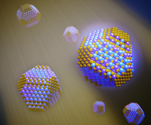
"Our calculations revealed that a homogeneous cation distribution would yield optimal solar cell performance in these disordered materials, corroborating the experimental discoveries as a testament of the synergism between theory and experiment.” (The picture above is an illustration of the homogenous cation distribution achieved inside the AgBiS2 nanocrystals)
With this result, they constructed an ultrathin solution-processed solar cell by depositing the AgBiS2 nanocrystals, layer-by-layer, onto ITO/Glass, the most commonly used transparent conductive oxide substrates, among others. They coated the devices with a PTAA (Poly triaryl amine) solution and upon illuminating the device under artificial sunlight, they recorded a power conversion efficiency in excess of 9 percent for a device with a total thickness no more than 100 nm, 10-50 times thinner than current thin film PV technologies and 1000 times thinner that Silicon PV.
One of the devices was sent to an accredited Photovoltaic (PV) calibration laboratory in Newport, USA, which certified a conversion efficiency of 8.85 percent under AM 1.5G full sun illumination.
Konstantatos says: “the devices reported in this study set a record among low-temperature and solution processed, environmentally friendly inorganic solar cells in terms of stability, form factor and performance. The engineering of the multinary systems with cation disordered AgBiS2 colloidal nanocrystals has proven to offer an absorption coefficient higher than any other photovoltaic material used to date, enabling highly efficient extremely thin absorber photovoltaic devices. We are thrilled with the results and will continue to proceed in this line of study to exploit their intriguing properties in photovoltaics as well as other optoelectronic devices”.
REF
'Cation disorder engineering yields AgBiS2 nanocrystals with enhanced optical absorption for efficient ultrathin solar cells' by Yongjie Wang et al; Nature Photonics, 2021


