Loading...
News Article

Innoscience delivers GaN HEMT for mobile handsets

News

40V bi-directional GaN HEMT with low RDS(on) targets smart mobile devices, chargers and adapters

Chinese GaN company Innoscience, has announced the INN40W08, a 40V bi-directional GaN-on-Si enhancement mode HEMT for mobile devices, including laptops and cellular phones. The INN40W08 HEMT has been developed using the company's InnoGaN technology.

Commented Denis Marcon, general manager of Innoscience Europe and marketing manager for the USA and Europe: "GaN technology has been adopted by manufacturers of mobile phone chargers over the last couple of years to deliver increased power and shrink device size. However, Innoscience's significant breakthrough now makes it possible to introduce GaN HEMTs into mobile phone handsets as well, increasing efficiency and performance. With Innoscience's huge available capacity, we provide the secure supply chain that customers nowadays expect."

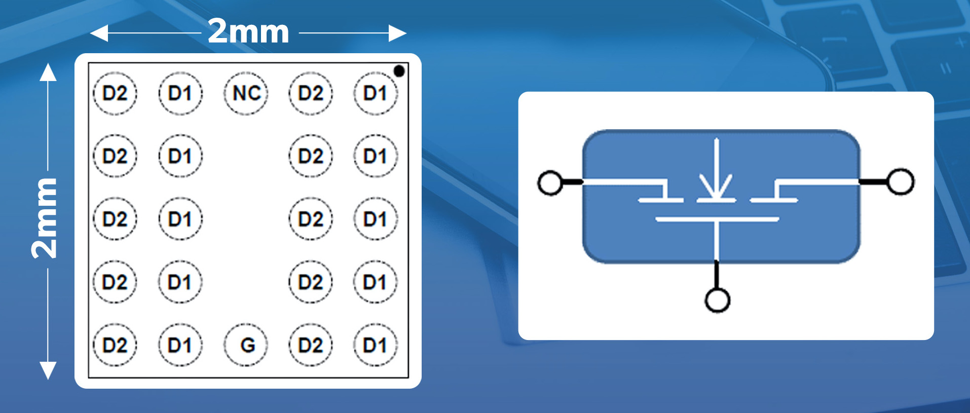
Featuring a bi-directional blocking capability, the new INN40W08 GaN HEMTs have an on-resistance of 7.8 mΩ. This is achieved by a patented strain enhancement layer technology which reduces sheet resistance by 66 percent. Gate charge (QG) is typically 12.7nC. The 5x5 grid wafer level chip scale package (WLCSP) measures 2x2 mm.

The small footprint enables INN40W08 GaN HEMTs to be integrated inside mobile phones. Applications include high side load switching, over-voltage protection in a smart phone's USB port and multiple power supplies including chargers and adapters. In over-voltage-protection systems, the technology can replace two silicon MOSFETs with one InnoGaN (or BiGaN) transistor.

Mitsubishi joins Horizon Europe's FLAGCHIP project
Vishay launches new high voltage SiC diodes
UK team leads diamond-FET breakthrough
GaN adoption at tipping point, says Infineon
BluGlass files tuneable GaN laser patents
QD company Quantum Science expands into new facility
Innoscience files lawsuit against Infineon
Riber revenues up 5% to €41.2m
Forvia Hella to use CoolSiC for next generation charging
Photon Design to exhibit QD simulation tool
Ortel transfers CW laser fabrication to Canada
Luminus adds red and blue multi-mode Lasers
PseudolithIC raises $6M for heterogeneous chiplet tech
Mesa sidewall design improves HV DUV LEDs
IQE revenue to exceed expectations
'Game-changing' VCSEL system targets clinical imaging
German start-up secures finance for SiC processing tech
Macom signs preliminaries for CHIPS Act funding
IQE and Quintessent partner on QD lasers for AI
EU funds perovskite tandems for fuel-free space propulsion
EU to invest €3m in GeSi quantum project
Transforming the current density of AlN Schottky barrier diodes
Turbocharging the GaN MOSFET with a HfO₂ gate
Wolfspeed launches Gen 4 SiC MOSFET technology
Report predicts high growth for UK's North East
Element Six unveils Cu-diamond composite
SemiQ launches hi-rel 1700V SiC MOSFETs
Lynred to exhibit Eyesential SWIR sensor for machine vision
Thorlabs buys VCSEL firm Praevium Research
Advancing tuneable InP lasers on a heterogeneous platform
P-GaN gate HEMTs have record threshold voltage
Guerrilla RF releases GaN power amplifier dice
×
Search the news archive

To close this popup you can press escape or click the close icon.
Logo
x
Logo
×
Register - Step 1

You may choose to subscribe to the Compound Semiconductor Magazine, the Compound Semiconductor Newsletter, or both. You may also request additional information if required, before submitting your application.


Please subscribe me to:


You chose the industry type of "Other"

Please enter the industry that you work in: