
Perovskite research offers new scope for solar cells
Los Alamos Lab exploration of 2D perovskite in device settings, yields promise for technology
In research published in the journal Chem, US Los Alamos National Laboratory researchers have examined the performance properties of two-dimensional perovskites in conditions representative of a device structure, finding those structures can be as efficient as their three-dimensional counterparts.
“We discovered that intrinsic to this material, there are some shallow defects or ‘trap states’ that can help the charge transport over a long distance,” said Wanyi Nie, researcher with the Center for Integrated Nanotechnologies group at Los Alamos National Laboratory. “The travel distance is slightly lower than three-dimensional perovskites, but is much greater than what people believed in a typical 2D quantum-confined system. So this is a critical finding that two-dimensional perovskites can be efficient as three-dimensional perovskites.”
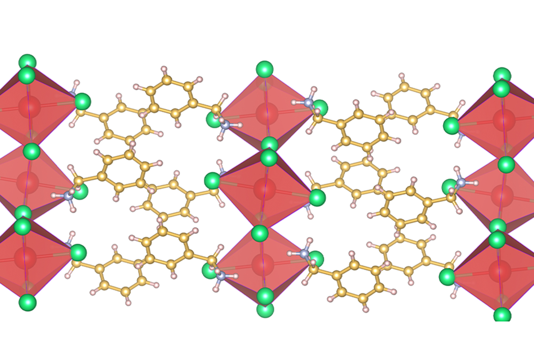
Three-dimensional perovskites are unstable under ambient environmental conditions. Layered structures can circumvent that environmental instability. However, poor charge conduction across the layers – the charge transport is hindered by the insulating spacer materials between the layers – has been a concern that caps the performance of these semiconductors.
To explore alternatives, Nie and the research team focused on the long in-plane carrier diffusion length in two-dimensional Ruddlesden-Popper (RP) perovskite crystals. Carrier diffusion length informs the length a charge can travel, with longer distances meaning greater efficiency and higher performance. The team probed the crystals via scanning photocurrent microscopy, in which a laser is trained on the material, relaxing it to allow electrons to reach nearby electrodes.
That technique provided a spatial mapping of photocurrents and explored optoelectronic properties. With the experimental setup including charge collection, interface and a mild electrical field, researchers were able to investigate the properties of the two-dimensional perovskite in a device structure for the first time. Visualizing the carrier diffusion in the presence of electrical fields provided observations of properties and performance directly relevant to the operation of a photovoltaic device.
Experiments showed that charge conduction can be enhanced by the two-dimensional perovskite’s intrinsic trap states: atomic-size defects in the material, sometimes shallow and sometimes deep. Those defects can result in long diffusion length, meaning photo-generated charges can travel longer and be collected as output electrical currents – the power supply for a device.
“The biggest challenge of this research from a fundamental perspective is that people have been observing this interesting phenomena of longer-than-expected diffusion length but couldn’t find the origin,” said Nie.
Surprising results in diffusion length offer promise for use in devices
Sergei Tretiak, chemical physicist in the Laboratory’s Theoretical division, led the theoretical modeling for the experimental system.
“We actually were surprised to see this kind of long diffusion length, longer than a micron, in a 2-dimensional system,” Tretiak said. “This corresponds to the most optimistic theoretical predictions for the charge lifetime and diffusion length assuming ideal 2D structures. That’s exciting because a longer diffusion length means the charge can actually be collected and used in a device.”
Nie and Tretiak hope to build on the discovery of the role of the shallow trap, leveraging the Laboratory’s unique theory and experimental framework established for 2D perovskite material systems to pinpoint the molecular origin of such defects. From there, the free carrier electron transport (the charge) can be manipulated by rationally designing the material structure, further tuning 2D perovskite properties viable for a span of electronic devices, such as photovoltaics, radiation sensors and information processors. Conversely, the shallow trap might also be reduced, leading to shorter diffusion length, which could be useful for lighting applications such as solid-state lighting or scintillators for X-ray imaging.
REF
'Long carrier diffusion length in two-dimensional lead halide perovskite single crystals' by Shreetu Shrestha et al; Chem.( Janiuary 2022)


