
P-n junction empowers GaN HEMTs
Adding a p-n junction to the GaN HEMT boosts its breakdown voltage
One of the most significant weaknesses of the commercial GaN HEMT is that its gate voltage tends to be limited to no more than about 7 V to ensure safe operation. This restriction reduces the choice of gate drivers and rules out the use of silicon-based designs that have a gate bias of more than 10 V.
To overcome this limitation, a Chinese collaboration between Nanjing University and CorEnergy Semiconductor has developed a novel, reliable, large-area device that offers robust control of the gate. This device combines a HEMT with a p-n junction.
According to team spokesman Feng Zhou from Nanjing University, the strengths of their proof-of-concept device, produced with industry standard processes, include a high breakdown voltage of 18.2 V and a capability to operate for a long time under a gate bias of more than 10 V. “This leads us to believe that the p-n junction HEMT can be used directly with silicon drivers.”
The Chinese partnership has been working on this novel GaN HEMT for several years, filing a patent back in 2019. “To our best knowledge, this is the first patent filed on the concept of the p-n junction gate architecture.”
Fulfilling this technology’s promise has not been easy, with the fabrication of large-area devices more challenging than their smaller counterparts, due to greater susceptibility to process variation.
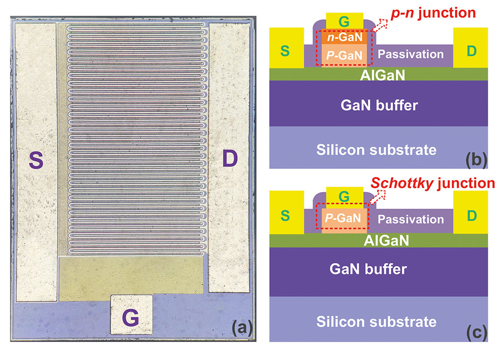
Recently, the team has overcome this, with recent efforts highlighting the strong performance of devices with an area of 4.9 mm2. These p-n junction HEMTs, along with a control that employs a Schottky junction, have been produced by taking a 150 mm silicon epiwafer, loading this into an MOCVD chamber, and depositing a 4.5 μm-thick buffer, followed by a 300 nm unintentionally doped GaN channel and a 13 nm-thick Al0.2Ga0.8N barrier layer. For the p-n junction HEMTs, a 100 nm-thick magnesium-doped p-type GaN layer is added, followed by a 40 nm-thick silicon-doped n-type layer.
To produce devices from these epiwafers, the engineers etch away the top p-type and n-type layers from the access region, prior to thermal activation of the remaining p-type material, and the addition of ohmic contacts for the source and drain. A 1 μm-thick SiN passivation layer is subsequently added, before removal of a window that allows the addition of the gate contact (see figure above which shows: (a) Optical image and cross-sectional diagrams of the: (b) GaN p-n junction HEMT and (c), the GaN Schottky-junction HEMT).
The team have deployed their p-n junction HEMTs in inductive switching circuits, where, compared with conventional Schottky-junction HEMT, they are said to deliver fast-switching and a strong immunity to dynamic on-resistance, . “What’s more, our device shows superior over-voltage reliability, with a record-high dynamic breakdown voltage of 1.62 kilovolts,” enthused Zhou.
Measurements of the dynamic blocking voltage have been undertaken with unclamped-inductive-switching experiments. Testing revealed an inferior value for 650 V Schottky-gate HEMTs of 1.45 kV. Having a higher value is very valuable, preventing the failure of power devices and the loss of all channel blocking capability due to gate failure.
An even better set of results could be realised, given that: the epitaxial material and the fabrication process are yet to be optimised, there is a degree of non-uniformity in the gate breakdown voltage, and there is hysteresis in the behaviour associated with the threshold voltage.
When analysing gate characteristics of unoptimised devices, the team found that the n-GaN capping layer in the gate stack plays a crucial role in suppressing the gate leakage current and tuning the electric-field distribution within the depletion region. This led them to see the need to improve material characteristics of the n-type GaN capping layer, such as its concentration and thickness, as well as its deposition conditions and gate-related fabrication processes.
“Additionally, our team is focused on optimising device packages for low parasitics,” revealed Zhou.
REF
F. Zhou et al. IEEE Trans. Power Electron. 37 26 (2022)


