

Optimising gallium oxide growth
How do you produce great gallium oxide power devices? It’s a combination of
excellent reactor design, ideal precursors and dopants, a partner
material for forming heterostructures, and good dielectrics and
contacts.
BY Fikadu Alema, Aaron Fine and Andrei Osinsky FROM
AGNITRON, Arkka Bhattacharyya FROM The University of Utah AND Sriram
Krishnamoorthy FROM UCSB
The global consumption of electricity, the most vital of all our energy sources, is sure to rise over the coming decades. So, in order to save the planet, it is critical to generate more electricity from renewables, and use this precious resource as efficiently as possible.
Efforts are already underway to trim the losses associated with transmitting electricity and its conversion from one form to another, such as from AC to DC. Savings are also coming from the increased adoption of wide bandgap devices, made from SiC and GaN. It’s certainly a step in the right direction, but even better results are possible by making power electronic devices out of an even wider bandgap material, β-Ga2O3. Compared with that pair of middleweights, it has a higher critical electric field and, at the system level, promises improvements to size, weight and power. What’s more, sizeable single crystals can be grown from the melt, enabling manufacture of devices on large native substrates that are cheap to produce – the same can’t be said for GaN and SiC.

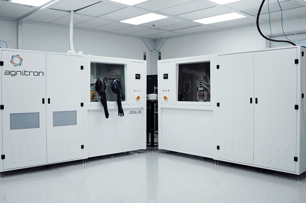
The Agnitron Agilis 100 is a single-wafer tool. Using induction heating, wafer carrier temperatures can reach up to 1,700 °C.
One big decision facing every developer of Ga2O3 power devices is which epitaxial process to employ. Films of β-Ga2O3 have been produced by MBE, HVPE and MOCVD, but there are strong arguments to suggest that the latter is the best growth technology for this oxide. For example, Ga2O3 grown by MOCVD has the highest low-temperature mobility – it is eight times higher than that for samples produced by MBE, and four times that for material made by HVPE (see Figure 1). It is also worth noting that the purity of epitaxial β-Ga2O3 films grown by MOCVD is higher than state-of-the-art values for 4H-SiC and GaN materials, which have been studied and refined for decades.
Additional attributes of MOCVD are that it is capable of producing high-quality, uniform epitaxial films with controllable doping levels at growth rates varying from just 0.1 mm/hr to as much as 10 mm/hr. Controlling the growth rate and the doping level makes MOCVD suitable for producing lateral and vertical devices, both geometries of interest for developers of power devices.
Even though Ga2O3 is still in its infancy, there is no need for companies or university groups that are keen to develop and refine Ga2O3 power devices to build their own reactors. Commercial tools are available, including those provided by those of us at Agnitron Technology of Chanhassen, MN. Since 2016 we have been actively developing MOCVD reactors to grow high-purity Ga2O3 and its related alloys for R&D and commercial applications. Over that time we have built and sold more than ten MOCVD reactors worldwide that are suitable for growing Ga2O3.
Our reactors have already produced record-breaking results, as confirmed at our internal R&D laboratory at Agnitron, and also by a number of our customers. Back in 2019, a collaboration between those of us at Agnitron and James Speck’s group at the University of California, Santa Barbara (UCSB), unveiled a record-breaking room-temperature electron mobility of 176 cm2 V-1 s-1 for unintentionally doped β-Ga2O3, grown using our Agilis 100 reactor. Since then, driven by remarkable improvements, both internally and by our customers, even higher mobilities have been reported. They include values for room-temperature electron mobilities from 140 cm2 V-1 s-1 to nearly 200 cm2 V-1 s-1, the theoretical limit for Ga2O3,by Agnitron, Krishnamoorthy’s group at the University of Utah (now at UCSB), and Zhao’s group at the Ohio State University (OSU) – both are using Agnitron’s Agilis 100 reactors (see table 1 for an overview of impressive results for mobility, both at room temperature and cryogenic temperatures).
The close working relationship between our team at Agnitron and a number of world-class researchers has supported the development of our growth reactors and processes. Operating in this manner, we have assembled a great deal of expertise associated with the growth of gallium oxide. We will now share this with you, offering our insights into the choices for the sources of gallium and oxygen, how best to dope this material, how to form a superlattice, and how to add dielectrics and contact materials. After covering all of this, we shall finish by detailing the merits of particular designs with Agnitron’s MOCVD portfolio.
Which gallium precursor?
Growers of epitaxial β-Ga2O3 films have two forms of gallium precursor to choose between: the more common tri-methyl-gallium (TMGa), and the variant tri-ethyl-gallium (TEGa). Having the upper hand in many regards is TMGa. This precursor has greater availability, thanks to its widespread use for growing various GaN-based and GaAs-based commercial devices; it is relatively low in cost; and it enables fast growth rates.
Using a close-injection showerhead reactor, we have realised a growth rate of around 10 µm/hr. Such a high growth rate shortens the time it takes to form epistructures with layers that are tens of microns thick, required to block voltages in excess of 10 kV.
Table I. Room-temperature (RT) and low-temperature (LT) Hall electron mobility data of β-Ga2O3 homoepitaxial films grown using various Agnitron MOCVD systems. TEGa/TMGa and pure oxygen/nitrous oxide (N2O) were used as gallium and oxygen sources, respectively. Also, RT free-carrier concentration(nRT) and accepter concertation (NA), showing the purity of the material, are presented. The table summarizes data reported both by Agnitron Technology and its customers.
The faster growth rate for TMGa, compared with TEGa, partly comes from a higher vapour pressure that enables the introduction of a higher concentration of gallium into the growth chamber. In addition, TMGa undergoes faster reaction kinetics. During pyrolysis, TMGa decomposes through a two-step mechanism, while for TEGa it is a three-step process. Shortening the reaction pathway allows TMGa to react faster with the oxidizing gasses, ensuring a higher growth rate. Mobility is also better with TMGa. According to our in-house study, low-temperature mobility for epitaxial b-Ga2O3 grown with the TMGa precursor is around 18,000 cm2 V-1 s-1 at 46K, rising to 23,400 cm2 V-1 s-1 at 32 K, compared with 11,700 cm2 V-1 s-1 at 46K for an epitaxial film grown using TEGa. This has led us to conclude that compared with TEGa, TMGa produces a higher purity film.
There are concerns with TMGa, related to carbon incorporation. How carbon behaves in Ga2O3 is debatable, but it is predicted to act as a deep donor state, with some research showing that it takes the form of a positively charged shallow donor. Preventing carbon from incorporating into Ga2O3 is not easy, given its presence in precursors. However, for TMGa, carbon incorporation can be enormous, due to the formation of highly reactive methyl radicals during the pyrolysis process. In contrast, decomposition of TEGa produces a stable ethylene group, which exits the reactor, lowering carbon incorporation.
The extent of carbon incorporation into Ga2O3 films grown by TMGa depends on the growth conditions. While significant incorporation can occur in an oxygen-deficient environment, optimised conditions are able to mitigate carbon contamination and yield high purity films. And for unintentionally doped Ga2O3, silicon impurity concentrations are ten times lower with TMGa than TEGa, explaining why film purity is better with the former precursor.
Nitrous oxide or oxygen?
When growing Ga2O3 films, one option for the oxygen source is nitrous oxide (N2O). This gas can also provide a nitrogen dopant, with variations in substrate temperature enabling nitrogen concentrations ranging from around 2×1019 cm-3 to a level undetectable by secondary-ion mass spectrometry. When incorporated in Ga2O3, nitrogen acts as a deep acceptor, producing semi-insulating material. Compared with films grown with an oxygen source, the free carrier concentration is much lower, an asset for making high-voltage vertical power devices.
If film purity is paramount, it is better to use pure oxygen. Measurements at 100 K show that electron mobility is around six times
higher for films grown with a pure oxygen source, rather than N2O.
Figure 1. (a) A comparison of the best low-temperature (LT) mobilities for films grown by MBE, HVPE and MOCVD. The MOCVD films are grown using Agnitron’s system at the Ohio State University (MOCVD/OSU), and Agnitron
Technology (MOCVD/Agni). MOCVD films were grown using either TEGa or
TMGa sources. (b) LT mobilities for TEGa/TMGa grown β-Ga2O3 films
compared with the state-of-art LT mobilities for 4H-SiC and GaN. It
should be noted that the MBE high mobility result was demonstrated in a
two-dimensional electron gas (2DEG) β-(AlxGa1-x)2O3/Ga2O3
heterostructure.
Forming heterostructures
The most obvious partner for Ga2O3 for forming a high-quality heterostructure is (AlGa)2O3. Using single-wafer and multi-wafer MOCVD reactors, we have developed processes for growing high quality (AlGa)2O3 alloys. We have produced a high-quality, strained single-layer β-(Al0.21Ga0.79)2O3/Ga2O3 heterostructure using our Agilis 700 MOCVD reactor (see Figure 2 for an X-ray diffraction pattern), as well as a superlattice with abrupt interfaces (see Figure 3). These successes are an important milestone, because the (AlGa)2O3/Ga2O3 heterostructure is a critical building block for various device structures, including HEMTs and modulation-doped FETs (MODFETs).
Figure 2. X-ray diffraction ω-2Φ scan profile for β-(Al0.21Ga0.79)2O3/Ga2O3 grown on a 2 inch (010) β-Ga2O3 Synoptics substrate by an Agilis 700 MOCVD reactor. The β-(Al0.21Ga0.79)2O3/Ga2O3 layer is 70 nm thick (XRD measurement was done at UCSB by Takeki Itoh from James Speck’s group).

Figure 3. X-ray diffraction (XRD) ω-2θ scan profile for
ab-(Al0.21Ga0.79)2O3/Ga2O3 superlattice (SL) grown on a 2-inch (010) β-Ga2O3 Synoptics substrate using an Agilis 700 MOCVD reactor. The SL
has eight periods and the thickness for the β-(Al0.21Ga0.79)2O3 barrier
and Ga2O3 well are 5 nm and 10 nm, respectively. Observation of
Pendellösung fringes in the XRD scan indicates the growth of a coherent
and smooth SL using commercial-scale MOCVD reactors (XRD measurement was
done at UCSB by Takeki Itoh from James Speck’s group).
The maximum aluminium content realised in the (AlGa)2O3 film depends on the orientation of the substrate. It is challenging to realise an aluminium content of more than 25 percent on (010) oriented β-Ga2O3, while this is relatively easy to reach without phase segregation with (-201) and (100) orientations. Zhao’s group at OSU have reported phase pure β-(AlGa)2O3 alloys with an aluminium content of up to 52 percent on a (100) β-Ga2O3 substrate using one of our reactors, and Krishnamoorthy’s group have realized MODFET structures using (AlGa)2O3 layers. Note that with other phases, such as ∝-(AlGa)2O3, phase pure alloys can be grown with aluminium contents from 0 percent to 100 percent.
Delivering doping
Thanks to the availability of suitable precursors in either a gas or metalorganic precursor form, silicon, germanium and tin can all be used to dope Ga2O3. However, silicon is favoured, due to its efficient incorporation and activation – and unlike germanium and tin, it does not have a memory effect in the reactor.

Figure 4.Electron mobility versus free-carrier concentration for silicon
(a) or germanium (b) doped β-Ga2O3 epitaxial films grown by MOCVD using
TEGa and TMGa precursors.
Using TEGa and TMGa, our studies have shown that with silicon as the dopant n-type conductivities can range from 2 x 1014 cm-3 to 3.4 x 1020 cm-3, compared with 2 × 1016 cm to 2.6 -3× 1020 cm-3 for germanium (see Figure 4). As well as the more limited doping range, germanium is impeded by a strong temperature dependence in stability in the film. When deep acceptor doping is needed, options include magnesium, iron and nitrogen.
Doping is even possible at low substrate temperatures, such as 600 °C. Work by those of us at Agnitron has demonstrated silicon doping in excess of 3 x 1020 cm-3, along with a record conductivity of more than 2500 S/cm. Use of a low temperature ensures a low thermal budget and permits both a masked contact regrowth process and in-situ dielectric deposition. Both have been used during device fabrication.
Ohmic contacts and dielectrics
Leveraging low-temperature epitaxy, Krishnamoorthy’s group has demonstrated MOCVD-regrown ohmic contacts when fabricating β-Ga2O3 MESFETs formed entirely by MOCVD. These transistors offer improved on-state performance, with an on current of 130 mA/mm and an on-off ratio of over 1010. The silicon-doped β-Ga2O3 regrown layers deliver exceptional performance, with a record low sheet resistance of 73 Ω/sq, and a record low contact resistance for the metal/β-Ga2O3 junction of just 8.3 × 10⁻⁷ Ω cm2. When collaborating with those of us at Agnitron, an even lower contact resistance of just 1 x 10⁻⁷ Ω cm2 has been realised, very encouraging for high frequency devices, which require low parasitic resistances.
Until recently, one weakness of the Ga2O3 device has been its inability to combine a high lateral figure of merit with kilovolt breakdown voltages. Making devices out of structures grown at Agnitron, Krishnamoorthy’s group in collaboration with us at Agnitron, overcame this challenge, reporting record-breaking results for lateral Ga2O3 MESFETs featuring a novel field plate design and produced with an improved contact regrowth process, developed at Agnitron. Measurements on a device with a gate-drain spacing of 10 mm revealed a record-high lateral figure of merit of 355 MW cm-2, a breakdown voltage of around 2.5 kV, and an average electric field at breakdown of about 2.5 MV/cm.
More recently, this group has realised new highs, with breakdown voltages in excess of 4 kV, for devices made of Agnitron structures with lateral figures of merit exceeding 100 MW cm-2 (results were measured in Uttam Singisetti’s group at the State University of New York at Buffalo). Such results showcase the huge potential of these devices for serving in low-to-medium-voltage power systems, which are deployed in power supplies, electric automation and vehicles, power transmissions, and electrical grid integration.

The multi-wafer Agilis GOX300 has a wafer loading capacity of
five-4-inch wafers. This tool, designed for high-volume production,
delivers repeatable, reproducible growth processes and ensures that
epiwafers have excellent deposition uniformity and minimal particle
count. Wafer carriers can be loaded into the system at any given time,
to enable efficient, steady-state campaign operations involving up to
four wafer carriers.
One of the tremendous advantages of an oxide MOCVD system is that, without having to break vacuum, it can be employed after the growth of the channel to deposit dielectrics that provide gate oxides. Krishnamoorthy’s group have adopted this approach, carrying out the entire process in-situ process – this eliminates the need for surface treatment and minimises the threat of contamination between epitaxial growth and dielectric deposition.
Measurements reveal an interface state density of around just 6.4 × 1011 cm-2 for the Al2O3/ Ga2O3 interface produced by in-situ growth, and breakdown fields of up to 5.8 MV/cm, a figure comparable to Al2O3 dielectrics grown by atomic layer deposition. Such results hold much promise for the future of β-Ga2O3-based high-performance MOSFETs.


Figure 5. Measurements of the layer thickness and surface roughness
highlight the uniformity and smoothness of the Ga2O3 epilayers. There is
a uniformity of 3 percent (1s) and RMS roughness of 0.8 nm.
Agilis MOCVD systems
Thanks to progress of Ga2O3 on many fronts – the ability to grow electronic-grade epitaxial films over a wide temperature window, the highly tuneable growth rates and doping levels, and the growth of alloyed single crystals and in-situ dielectrics – we can expect an increase in the research, development and prototype production of devices in the coming years. To support such efforts, we are offering four families of MOCVD reactor designed for the growth of β-Ga2O3: the Agilis 100, 500 and 700; and the GOX300 series.
Of these, the Agilis 100 is a single-wafer reactor, accommodating one substrate up to 3 inches in diameter; the 500 and 700 house up to five and seven 2-inch wafers, respectively; and the GOX300 can cater for up to five 4-inch diameter wafers. All systems come with our record-setting recipes/processes and decades of stress-free, low-cost future equipment support and maintenance. Every model can be configured to match individual requirements, budget, and facility constraints.
The Agilis 100, an ideal research tool, has recently been updated to accommodate larger wafers and a faster rotation speed of up to 1,500 rpm. It can be configured with our brand new close-injection showerhead gas distribution system, or it can employ a remote-injection showerhead. Using induction heating, wafer carrier temperatures can reach up to 1,700 °C.
The multi-wafer Agilis 500 and 700, which share the same compact footprint of the 100, are also capable of wafer rotation at up to 1,500 rpm. Both use a close-injection showerhead to minimize the gas phase reaction of precursors. Resistive heating is employed, with the option of selecting multi-zone heaters with active temperature, drawing on measurements from either emissivity compensated pyrometry or thermocouples. Uniformity is excellent (see Figure 5), with epilayer root-mean-square surface roughness between 0.5-0.8 nm, which is within the range needed for lateral channel device structures.
If versatility is paramount, we recommend our dual-module systems, formed by combining two separate Agilis systems via a vacuum transfer mechanism. As well as growing β-Ga2O3, these vertical reactor geometry systems can deposit other materials, including III-nitrides, SiC, MgZnO, phosphorene, 2D BN, and the family of transition metal dichalcogenides, such as MoS2, MoSe2, WS2 and WSe. Such a wide range of materials is easy to realise, thanks to the opportunity to fit up to 12 metal-organic sources, which can be switched within minutes.
Large-scale production
In response to the growing market demand, those of us at Agnitron have started offering multi-wafer Agilis reactors. The latest addition to this range, the multi-wafer Agilis GOX300 with a wafer loading capacity of five-4-inch wafers, also deliver repeatable, reproducible growth processes and ensures that epiwafers have excellent deposition uniformity and minimal particle count.
With this system, wafer carriers can be loaded into the system at any given time to enable efficient, steady-state campaign operations involving up to four wafer carriers. Transfer is provided with an industry-standard automated robotic arm operating in a high-vacuum transfer chamber. Dwell stations are used for loading and unloading platters of wafers.
The Agilis GOX300 features our proprietary, highly developed rotating disc reactor (RDR) vertical growth chamber. In this chamber, flow dynamics repress recirculation, leaving sensitive areas above and around the wafer carrier clean and free of deposition. The RDR is a proven success, having already been implemented in our A300 series that’s designed for growing arsenides and phosphides.
Thanks to the launch of our Agilis GOX300, we have strengthened our suite of tools for the development and production of gallium oxide devices. Supported by our reactors and knowhow, pioneers of this oxide can take power electronics into a new era, building on the benefits wrought by GaN and SiC, and driving down losses on electrical systems to unprecedented levels.
Further reading
F. Alema et al. Journal of Crystal Growth 475 77 (2017)
G. Seryogin et al. Applied Physics Letters 117 262101 (2020)
Y. Zhang et al. APL Materials 7 (2019) 022506.
R. Miller et al. Compound Semiconductor Magazine 24 (4) 18 (2018)
A. Bhattacharyya et al. IEEE Electron Device Letters 42 1272 (2021)
F. Alema et al. APL Materials 7 121110 (2019)
F. Alema et al. MOCVD Growth of β-Ga2O3 Epitaxy, in: J. Speck & E. Farzana (Ed.), “β-Ga2O3: Wide-bandgap Semiconductor Theory and Applications”, American Institute of Physics 2022
F. Alema et al. APL Materials 8 021110 (2020)


