

Monitoring methane with 3D single-pixel imaging
A novel camera with a single-pixel detector that’s operating in
photon-counting mode is set to revolutionise detection and tracking of
methane, a troublesome greenhouse gas
BY JOLYON DE FREITAS AND
NICHOLAS AVLONITIS FROM THE CSA CATAPULT, DOUG MILLINGTON-SMITH AND
MURRAY REED FROM QLM AND SIMON DIMLER AND JO-SHIEN NG FROM SHEFFIELD
UNIVERSITY
MULTI-PIXEL SENSORS are a great commercial success. Aided by their low-cost and large-scale manufacture they are benefitting from a technological ‘lock-in’, along with a dependence that is difficult to escape.
Underpinning the meteoric rise of this imaging technology, particularly for digital imaging, is the single-pixel detector. Its origins can be traced back as far as 1965, when the American engineer Frederic Crockett Billingsley used the term ‘pixel’ for the first time in the context of the picture elements of scanned images. Today, though, this term is used interchangeably – it can mean either the smallest indivisible image element, or the smallest independent sensor element of an array. When a single pixel is used for imaging, it is combined with some form of scanning – this is the approach that has been adopted almost exclusively in low-photon-count situations, both within and outside the visible spectral range.
Several forms of single-pixel optoelectronic device are now available, including photomultiplier tubes and single-element semiconductor devices, such as detectors based on either silicon, germanium or InGaAs. Since the 1970s these detectors have been behind the digital medical imaging revolution in X-ray computed tomography (CT), nuclear medicine, positron emission CT and more recently photon-counting CT. These instruments have transformed healthcare, biology, quality engineering, defence and several manufacturing industry sectors.
Against this backdrop, saying that single-pixel imaging is new might appear to be a contradiction in terms. But that’s not the case: single-pixel imaging is not just new, it is radically new. The reality is that, like the radically new approaches of medical imaging in the 1970s, single-pixel photon imaging is on the cusp of a new era. What’s more, the similarity in trajectory doesn’t end there: single-pixel imaging is now realising a true 3D spatial reconstruction of the object scene thanks to a time-of-flight capability. Normally this is accomplished with light detection and ranging (lidar), a technology that determines the shape of an object.
As well as these new developments, single-pixel imaging is finding niche applications in the short-wave infrared (SWIR), particularly when there is a need for single-photon counting detectors. Such devices are made from either InGaAs/InP, InGaAs/InAlAs or germanium/silicon. These semiconductor detectors can monitor greenhouse gases, support environmental management and help to assess whether regulations are upheld.
For environmental monitoring and gas sensing, compound semiconductor technologies have much appeal. Their merits include enabling the engineering of smaller bandgap energy levels, suitable for the absorption and detection of lower-energy photons. By reaching down to the short-wave and medium-wave infrared, detectors can delve into a spectral domain rich in distinctive vibrational and rotational spectra associated with many greenhouse gases.
The case for methane
Reducing greenhouse gases is key to realising a zero-carbon economy. To get there demands regulation and enforcement, as well as focusing on what matters. While it’s easy to get fixated on CO2, the biggest greenhouse gas, it is folly to neglect other global greenhouse gases. This includes methane, the second biggest greenhouse gas. This hydrocarbon is the main constituent of natural gas, which is seeing increased demand as nations move away from coal and oil. One of the main reasons why methane emissions really matter is that over a 20 year period from their release, they trap 84 times more heat than comparative emission of CO2. Due to this, it takes just a 3 percent leak rate to make natural gas as bad for climate change as burning coal.
One of the more pleasing outcomes at COP26 has been a commitment signed by more than a hundred nations to reduce their methane emissions. However, you cannot manage what you cannot measure; and that’s a big issue, because today there appears to be no proper measurements of methane sources and fluxes. If this is addressed, then as well as tackling the environmental cost associated with methane, financial losses will tumble. According to independent research provider Rhodium Group, leaks of methane are valued at more than $30 billion per year. Due to this, there is a substantial, growing market for natural gas leak detection.
In 2018, the analyst Research and Markets estimated that this market is worth more than $1.5 billion, and increasing at a compound annual growth rate of more than 7 percent, due to a combination of gas becoming the dominant fossil fuel, slowly increasing government regulations, and expanding investor pressure to drive up industry standards.
Unfortunately, today’s detection technologies are complex, expensive and need trained experts to operate. Consequently, regulations are only enforced after occasional inspections. It’s a state of affairs that concerns the gas industry: it wants to find ways to catch these leaks, and ensure that gas suppliers are environmentally responsible and worthy of investment. Success on all these fronts will help to reinstate natural gas as a transition fossil fuel.
For those that are willing to devote time and energy into developing methane monitoring systems, the commercial opportunities do not begin and end with methane production and supply. There is also the petrochemical industry, which consumes natural gas to manufacture a wide range of industrial materials.
The 2,000 chemical plants worldwide have created a gas leak detection market worth $0.5 billion and tipped for substantial growth, due increasing safety regulation, as well as interest from other major industries, such as construction and transport. Additional opportunities exist in environmental monitoring of innovative landfill-gas-to-energy and anaerobic digestion plants – they need improved greenhouse-gas leak detection.
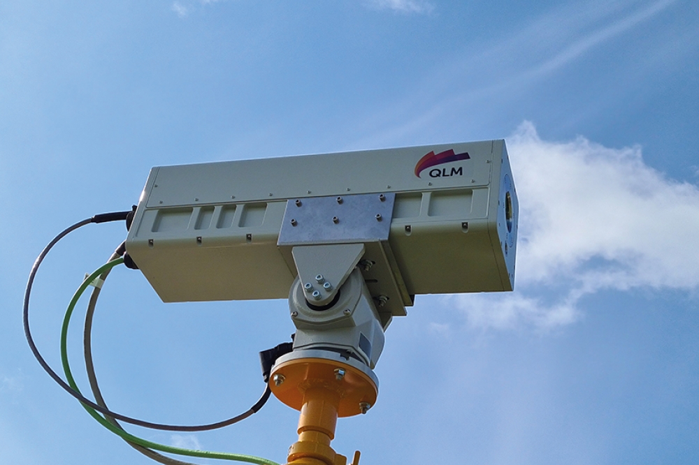
Figure 1. Left: QLM’s TDLidar single-pixel 3D gas imaging camera. Right: Multi-dimensional image of methane gas leak detection and distance information. Images conjured up by the TDlidar camera.
A UK solution
Supported by InnovateUK, we are involved in a collaboration that is part of a project entitled SPLICE – an acronym for Single Photon Lidar Imaging of Carbon Emissions – that is targeting the practical detection of methane. Drawing on quantum technology pioneered by the University of Bristol, our team from the Compound Semiconductor Applications Catapult (CSA Catapult), QLM and Sheffield University, is developing disruptive infrared lidar cameras that offer real-time imaging and quantification of greenhouse gases at long range, giving industry what it needs: an accurate, low cost and practical leak detection system that can completely and continuously survey greenhouse-gas emissions. Additional partners in SPLICE include the National Physical Laboratory, and gas industry leaders BP and National Grid Gas.
Figure 2. Design objectives of a typical InGaAs/InP single-photon avalanche diode (SPAD) design using the SAGCM – Separate absorption, grading, charge and multiplication approach.
We are aware that accurately measuring methane emissions is a tricky task. Take a plant, for example, which will have a wide variety of sources of emission: there are vents and exhausts, which are large, localised and planned; there are flares, which are large and localised, but often unplanned and intermittent; and there are fugitive emissions – leaks – that are small, widely distributed, and often unknown until found. Due to this complexity, emissions tend to be estimated rather than measured. This involves the use of simple multipliers and the prediction of emissions based on ideal conditions, a method that can lead to wildly inaccurate results. Another concern is that when leak detection and repair operations take place, they are slow, expensive, labour intensive, and only provide a snapshot in time of the facility. If a component springs a leak the day after the survey, this issue only surfaces during the next survey, months down the line.
The obvious solution is to continuously monitor methane. However, that’s not as simple as it sounds. One low-cost option is to install a network of point sensors – but this requires regular calibration and offers little effective localisation or quantification. An alternative, the optical gas imaging camera, addresses the former by visualising emissions with infrared thermal imaging, but it is also weak in terms of quantification. Better in that regard is open path spectroscopy, which uses the atmosphere as the measurement cell, but this trades quantification for localisation. Yet another option is to use imaging from satellites. This approach visualises and quantifies, but monitoring is intermittent, thwarted by clouds, and spatial resolution is limited to no more than a 25 m square.
None of these candidates provides the total package of continuous detection, localisation and quantification that is craved by the gas industry, which faces an immense problem. Consider the following: in North America alone there are 2,000 offshore rigs; worldwide there are nearly 1,000 natural gas storage facilities; and in Britain there are 24 major pipeline compressor stations and hundreds of above-ground installations, all leaking to some degree right now.
Well aware of these issues, oil and gas majors are making various pledges to reduce methane emissions over the coming decades. Among those leading this drive is SPLICE Project Partner BP, which has committed to monitoring methane at all its major sites by 2023. This should enable a 50 percent cut in methane emissions intensity, prior to realising full net zero in 2050.
It is likely that many other gas providers will follow, partly because in recent weeks the US Environmental Protection Agency has proposed changes to monitoring regulations that will lead to more regular reporting. This environmental agency is also making allowances for measurements with new, non-standard technologies. Should this proposal become law, it will grant US-based emitters a range of options for helping to meet more stringent standards.
Conjuring images
Within our collaboration, QLM is addressing the needs of the gas industry by using a revolutionary quantum technology to deliver a true measurement of greenhouse gas emissions. This is accomplished with a camera that simultaneously visualises and quantifies plumes in real time. The approach that’s taken builds on some of the key advantages of previously described technologies while avoiding their limitations.
Our new sensor employs a technique called tuneable diode lidar (TDlidar). This enables remote spectroscopy and ranging with low-power semiconductor diode lasers, by drawing on aspects of tuneable diode laser absorption spectroscopy, with differential absorption lidar (DIAL) and time-correlated single-photon counting.
Initially, our TDlidar methane sensors employed diode lasers with wavelengths around the methane absorption line at 1650.9 nm, and Peltier-cooled single-photon avalanche diode (SPAD) detectors in a random modulation CW lidar system (see Figure 1). With this approach we could realise long-range, accurate imaging of gas uncovered by DIAL, using a much smaller, easily portable form factor.
This prototype has much appeal, promising simple, robust, precise visualisation and quantification of gas emissions on a continuous basis, from a compact, relatively low-cost platform. However, there is a massive difference between demonstrating technology on a laboratory bench and delivering a reliable, environmentally robust, simple-to-operate camera that will add value to real-world operations. Bridging that gap demands improvement to the internal workings of the camera, the mechanical operation and the control and analysis software; and proving that the equipment is at least as good as existing techniques when working in real environments.
On its own, QLM does not have all the skills and experience to tackle this multi-faceted challenge that includes handling multi-dimensional information in images conjured up by the camera. It is a different story, however, once QLM has teamed up with project partners that include CSA Catapult, Bay Photonics, and the Universities of Bristol, Sheffield and Aston. Another partner is STL Technology, which has developed software processing that turns measurements of spectra to representations of methane intensity. Through ergonomic design, our collaboration’s camera is evolving towards smaller, lighter, more affordable platforms.
Support from the SPLICE programme has helped us evaluate the performance of the camera. Initially, trials took place in controlled release settings, but more recently, as the camera has reached higher levels of readiness, trials have moved on to real-world environments. This has involved using the camera to hunt for leaks that are unknown to the operator, on test beds from both inside and outside the consortium.
Much progress has been made. QLM has already completed trials with SPLICE partner National Grid Gas, and trials are planned with other industrial partners of the project, AMETEK Land and BP.
Playing a very valuable role in supporting this evaluation of the camera has been another SPLICE partner, the National Physical Laboratory. Its scientists are providing test beds for controlled studies and comparative metrology during real-world trials. The insights garnered from this have allowed us to industrially validate the performance of our camera against state-of-the-art survey techniques.
Improving detection
At the heart of our single-pixel camera is a photon-counting detector operating in the SWIR. While SPADs in the visible region have seen significant advances, their cousins operating in the infrared are far less common, and do not always meet the performance requirements of the single-pixel camera. To address that shortcoming, those within our team at Sheffield University are designing and fabricating SWIR SPADs that are targeting higher detection efficiencies and a lower operational noise.
The most common form of SWIR SPAD involves InGaAs and InP. Photons are absorbed in a layer of InGaAs, while InP acts as the avalanche material. However, some research groups switch InP for lattice-matched In0.52Al0.48As, as this improves the temperature stability of the detector. An alternative material system for a SWIR SPAD is the combination of a germanium absorber and a silicon avalanche region. However, germanium’s indirect bandgap of around 0.8 eV prevents detection beyond about 1.5 μm.
Comparing the numerous SWIR SPADs that have been reported is far from easy, due to variations in the methods of characterisation. This includes differences in quenching methods; and for pulsed operation, variations in pulse duration, the levels of over-bias, and the photon detection efficiency. However, despite these challenges, we have attempted to summarise the typical range of values for some key performance characteristics for SWIR SPADs (see in Table 1).
Table 1: Comparison of typical 1550 nm single-photon avalanche diode (SPAD) specifications.
A key figure of merit for the SWIR SPAD is the photon detection efficiency. Specification for this tends to dictates the design of the device’s heterostructure. The photon detection efficiency is a product of the SPAD’s quantum efficiency and its breakdown probability – both can be increased, independently, by selecting a thicker absorption region and a thicker avalanche region, respectively. However, while this is true in theory, there are practical considerations. For example, thicker avalanche and absorption regions lead to a higher operation voltage, which may be undesirable.
Regardless of the material combination employed for the SWIR SPAD, its design must realise the desired electric field profile. Getting this right ensures that at the device’s operating voltage the field in the avalanche region is high enough to realise breakdown, a condition that ensures the detection of a single photon. Another key consideration is maintaining a low electric field in the absorber, which has a lower bandgap than the avalanche material, as this prevents excessive dark currents due to band-to-band tunnelling. To manage the large difference between the electric fields in the avalanche and absorber regions, inserted between them is a charge layer, sometimes referred to as a field-control layer (see Figure 2).
Production of InGaAs/InP SPADs usually involves the growth of the heterostructure by MOCVD, because this approach is already well-established for commercial manufacture of InGaAs/InP APDs originally developed for optical communication. Note that the zinc diffusion technique applied to form p-doped InP in those commercial APDs can be applied to InGaAs/InP SPADs.
For research projects targeting the mid-technology readiness level, or having a focus on translational research, such as our project that forms part of SPLICE, there are several good reasons why it is best to opt for semiconductor wafer foundries for the wafer source, assuming money is available for this work. During the pandemic, this approach has become even more advantageous, due to the long closures in university research labs in 2020, and the reduced capacity in both that year and 2021. Today, universities are dealing with a significant backlog of multiple experimental projects.
However, turning to a foundry is not always a problem solved. One issue is that they may decline the opportunity, viewing the number of wafers that are ordered as insufficient for the business model. And this may not be resolved by simply approaching other foundries, until one takes the order. Even before the pandemic, very few fabs were offering foundry services, and it is challenging for them to scale up, despite strong demand.
Figure 3. Schematic layout of the CSA Catapult’s SPAD testbed. The beam incident on the SPAD active area is adjusted using a beam profiler and a reference detector (Adapted from ETSI GS QKD 011 V1.1.1 (2016-05), GROUP SPECIFICATION: Quantum Key Distribution (QKD); Component characterization: characterizing optical components for QKD systems, May 2016).
Counting in the fog
It is a tricky business to characterise SWIR SPADs. As the photons are inherently random, there’s a need for a statistical approach. Complicating matters, only a few centres are equipped with the instrumentation to carry out these measurements. To help improve this situation, those within our team at the CSA Catapult have developed a SPAD testbed based on the ETSI Group specification QKD 011. This will help companies test different parameters of SPADs – clearing the statistical fog.
This testbed, illustrated in Figure 3, involves a weak laser source. Attenuation ensures that the source provides a 0.1 photons/pulse level on the SPAD’s surface. A multi-channel time tagger captures precise timings of arrivals of single photons, allowing the calculation of parameters based on statistics. With this testbed, methods have been developed to measure: the current versus voltage (I-V) characteristic, in order to identify the voltage thresholds; the dark count rate; the photon detection efficiency; and the probability of afterpulsing. Repeating measurements at different temperatures, set by the thermo-electric controller, enables this technique to examine the thermal effects on SPAD structures.
Drawing on the insights provided by the resulting range of measurements, design engineers can select the best components for their applications. In addition, measurements can aid the fine tuning of single-photon (quantum) imagers and sensors. Within the SPLICE programme, engineers have derived tremendous benefit from examining the effects of temperature on SPAD structures at different key wavelengths. This has assisted methane and greenhouse gas sensing (see Figure 4).

Figure 4. Left: The average number of photons falling on the single-photon avalanche diode (SPAD) active area can be reduced in a controlled manner to below an average of 0.1 photons per pulse. Right: Photodetection efficiency (PDE) of SWIR SPADs decreases with increasing temperature.
Multiple milestones
Throughout the project, we have faced many technical and logistic challenges. The pandemic has shut facilities, applied the brakes to global travel, and severely disrupted component supplies and collaborations. Yet despite all these difficulties, we have made strong progress on all our major objectives; and thanks to this progress, we are now fielding high-performing, robust, and user-friendly gas lidar imagers in multiple industrial field trials.
Our quantum systems depend critically on the SPAD detector. We continue to face a major challenge in procuring commercially available SPADs and characterising their performance for gas sensing applications. In it essential to know the area of the SPAD, its dark count rate, photon count probability, operating temperature, and applied voltage.
Championing efforts to understand and prove SPAD gas-imager requirements has been the team at CSA Catapult, which has also set the targets for the design of novel InGaAs-based SPADs by Sheffield University. This has led to the growth of the first SPAD device wafers, with efforts now directed at device fabrication and characterisation, to verify these designs. The best devices emanating from the University of Sheffield will soon be packaged in a form that allows their demonstration in prototype gas imager systems made by partner Bay Photonics.
We have no doubt that the trajectory of development of single-pixel compound semiconductor detector technologies will follow that of medical imaging of five decades ago. This is likely to lead to 4D imaging – that’s three spatial dimensions, plus time – along with real-time monitoring of gas plumes, newer ways of image registration and display of multi-dimensional information, and the development of fast, low-noise, multi-pixel photon-counting arrays. We are on the cusp of a revolution.
Further reading
G Gibson et al. Optics Express 25 2998 (2017)
G Gibson et al. Optics Express 28 28190 (2020)
A Mitchell et al. Environ. Sci. Technol. 49 3219 (2015)
ETSI GS QKD 011 V1.1.1 (2016-05), GROUP SPECIFICATION:
Quantum Key Distribution (QKD); Component characterization:
characterizing optical components for QKD systems, May 2016.


