
Slashing killer defects in gallium oxide
Third-generation gallium-oxide 100 mm epitaxial wafers with ten times fewer killer defects offer much promise for the commercialization of 100-A-class gallium oxide power devices
Novel Crystal Technology, working on commercial development of β-Ga2O3 Schottky barrier diodes in NEDO's "Strategic Energy Conservation Technology Innovation Program", has developed a third-generation gallium-oxide 100 mm epitaxial wafer in collaboration with Saga University. In this development, Novel Crystal Technology and Saga University improved the epitaxial wafer manufacturing technology and reduced the number of killer defects to one-tenth of that of conventional wafers. Such defects degrade the breakdown-voltage characteristics and have hindered efforts to increase the current of gallium oxide power devices.
This development makes it possible to commercialize the use of gallium oxide in 100-A-class power devices required by trains, industrial equipment and electric vehicles, and will lead to progress in energy saving and carbon neutrality.

Figure 1.(a) Film thickness distribution and (b) donor concentration distribution of third-generation β-Ga2O3 100-mm epitaxial wafer
During the few years, gallium oxide (β-Ga2O3) has started to attract much attention as a new material for low-cost power devices with low power loss. Power devices are used to control voltage and current in all types of electrical equipment from home appliances, automobiles, and trains to industrial equipment. Conventional power devices have been made from silicon, but suffer from power loss during power control. With the goal of reducing this loss, power devices made of SiC and GaN are being developed by various organizations. β-Ga2O3 is an attractive alternative to SiC and GaN because it enables the power loss to be further reduced and the power consumption of the equipment to be reduced. In addition, β-Ga2O3 can be expected to be economical because its manufacturing method is faster than that of SiC or GaN. For these reasons, research and development aimed at early commercialization of β-Ga2O3 power devices is currently underway in Japan and overseas.
Against this backdrop, Novel Crystal Technology and Saga University have been working on commercial development of β-Ga2O3 Schottky barrier diodes in NEDO’s (New Energy and Industrial Technology Development Organization) Strategic Energy Conservation Technology Innovation Program. By improving the manufacturing technology of β-Ga2O3 epitaxial wafers, they have managed to reduce the number of killer defects that degrade the breakdown voltage characteristics of the device to one-tenth of that of the current generation of β-Ga2O3 100 mm epitaxial wafers. Moreover, they have recently succeeded in developing a large-scale 300 A to 500 A-class gallium-oxide Schottky barrier diode. This new diode will make it possible to deploy 100 A-class β-Ga2O3 power devices in a wide range of markets, such as electric vehicles. The energy-saving effect of this development in the 2030s is expected to be more than 100,000 kL worth of crude oil per year, and major progress is expected toward achievement of carbon neutrality by 2050.

Figure 2 Current-voltage characteristics of (a) forward direction and (b) reverse direction of Schottky barrier diode
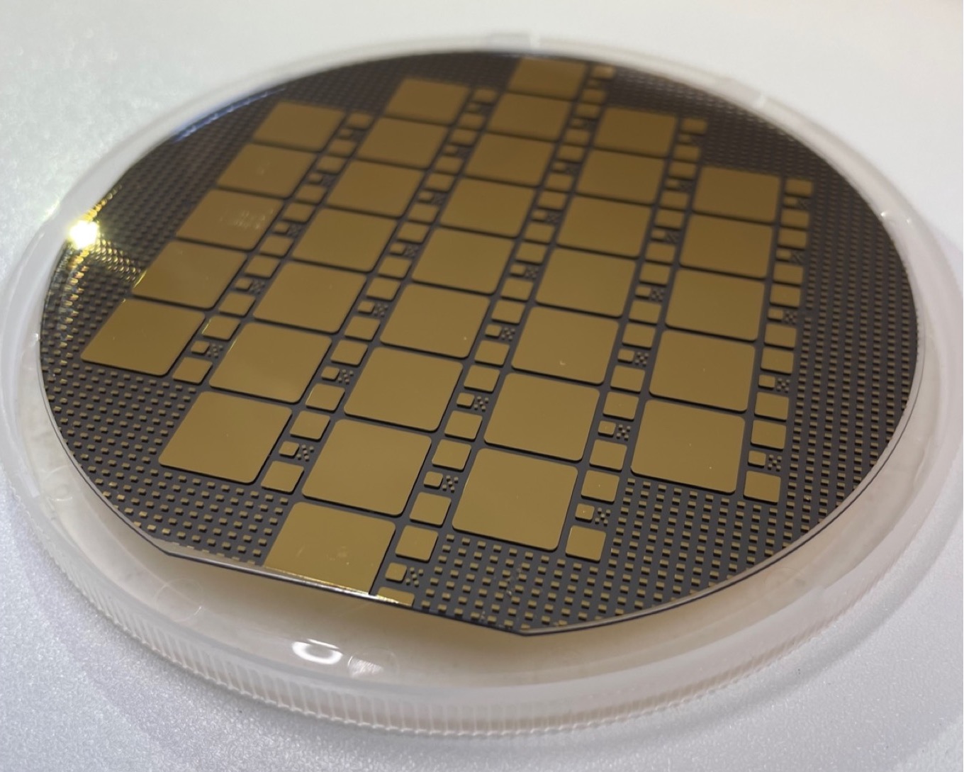
Novel Crystal Technology previously developed a second-generation of epitaxial-deposition equipment for scaling up the size of β-Ga2O3 epitaxial wafers to 100 mm, which are now being manufactured and sold as wafers. However, this sort of wafer has about 10 killer defects / cm2 that degrade the breakdown voltage characteristics of the device, meaning that these wafers can’t be used to make large devices and the current is limited to about 10 A. Through its collaboration with Saga University, Novel Crystal Technology has determined that the cause of the killer defects is a specific powder that is mainly generated during epitaxial deposition. By improving the epitaxial-deposition conditions, Novel Crystal Technology has developed a third generation of β-Ga2O3 100 mm epitaxial wafer with a killer defect density of only 0.7 pieces / cm2, which is less than one-tenth that of the second generation.
Success came from investigating the film thickness distribution and donor concentration distribution of the third generation β-Ga2O3 100-mm epitaxial wafer prepared under improved conditions (results are shown in Figure 1). Epitaxial wafers for power devices require a high uniformity of film thickness and donor concentration as well as low killer defect density. The film thickness distribution and donor concentration distribution measured at nine points on the epitaxial wafer plane were very small, about 10 μm ± 5 percent and 1 × 1016 cm-3 ± 7 percent, respectively. These levels are about one-seventh of those of the second-generation epitaxial wafers and present no problems for power devices.
Efforts continued with the prototyping of a β-Ga2O3 Schottky barrier diode on the new epitaxial wafer and the evaluation of its electrical characteristics and killer defect density. The largest electrode pattern on the wafer surface is the 10 mm × 10 mm β-Ga2O3 Schottky barrier diode.
Forward characteristics (see Figure 2 (a)) reveal that the current starts to flow from about 0.8 V and rises steadily and that normal forward characteristics are obtained. While the maximum current is 50 A, due to the limitation of the equipment (prober) used for this measurement, device current can flow a maximum of 300 to 500 A.
Reverse characteristics (see Figure 2 (b)) reveal that the leakage current can be suppressed to about 10-7 A even if about 200 V is applied. In the future, it is estimated that a breakdown voltage of about 600 to 1200 V can be obtained by incorporating an electrode termination structure into the device.
The reverse characteristic yield of the prototype diode is 51 percent, and the killer defect density is estimated to be about 0.7 pieces / cm2 from this value and the electrode size. This means that 100-A-class β-Ga2O3 power devices can be manufactured with a yield of about 80 percent.
Novel Crystal Technology will launch a new third-generation β-Ga2O3 100-mm epitaxial wafer production line and start selling its wafers in the near future. It will continue to work to reduce killer defects even further and increase the wafer diameter while expanding the available range of donor concentrations and film thicknesses. In NEDO’s project, Novel Crystal Technology has already succeeded in demonstrating a β-Ga2O3 Schottky barrier diode with a trench structure and a small power loss of 1200 V breakdown voltage. Novel Crystal Technology will continue to create mass-production technology for pressure-resistant trench-type Schottky barrier diodes by using the products it will develop in the future.
NEDO aims to realize sustainable energy conservation that is compatible with economic growth. As described in its “Energy Conservation Technology Strategy", development efforts such as this one will lead to commercialization of technologies that will have significant energy-saving effects in the 2030s in the energy, industry, consumer, and transportation sectors.


