
Superlattice thwarts degradation in dynamic on-resistance
Superlattices are superior to step-graded buffers at supressing degradation of dynamic on-resistance in GaN-based power devices
A team from China has shown that an AlGaN superlattice is better than a step-graded heterostructure at quashing dynamic on-resistance in GaN-based power devices.
According to the spokesman for the team, Xuelin Yang from Peking University, addressing degradation in dynamic on-resistance is critical because it impairs the performance and the reliability of power devices. “From the viewpoint of application, we need a stable on-resistance.”
Efforts by Yang and colleagues from Peking University, working in collaboration with researchers at Beijing University and the Collaborative Innovation Centre of Quantum Matter, have shed new light on a debate concerning the most appropriate architecture for reducing strain and ultimately quashing dynamic on-resistance degradation in GaN-based power devices.
Views expressed within the debate include claims that leakage paths only alleviate the degradation in the dynamic on-resistance, rather than suppress it; that the strain relief layer impacts depletion in the two-dimensional electron gas; and that the strain-relief layer influences the trap density. Other teams, however, see the strain-relief layer as an ideal dielectric, and are more concerned with the role of the carbon-doped buffer that sits on top, employed to boost the breakdown voltage. Extensive experiments by Yang and colleagues are now offering new insight – their investigations show that by providing more-effective blocking of electrons and holes, the superlattice is superior to the step-graded buffer at supressing degradation of the dynamic on-resistance.
The Chinese team came to this conclusion after comparing devices with step-graded and superlattice strain-relief layers. Both types of device had heterostructures grown by MOCVD on p-type silicon (111) substrates and featured a back gate on their underside and ohmic source and drain contacts separated by 15 μm. The device with the step-graded layer had a static on-resistance of 8.48 Ωmm, while the superlattice variant measured 9.09 Ωmm.
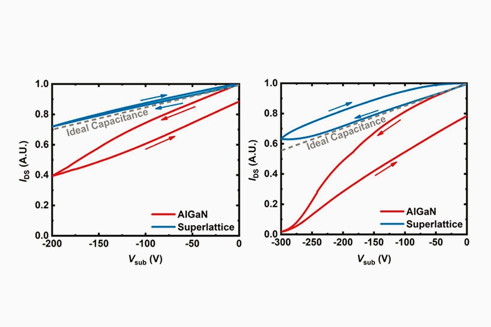
To uncover the influence of step-graded and superlattice structures on dynamic on-resistance, Yang and co-workers carried out back-gate ramping measurements. This study, revealing the impact of buffer trapping on the density of the two-dimensional electron gas in the channel, involved applying a fixed voltage of 0.5 V to the drain contact and sweeping a voltage applied to the back gate. If the entire epitaxial stack were an ideal dielectric without traps, it would behave as an ideal capacitor; but if there are traps in the buffer, charges would accumulate during this back-gate sweeping process, leading to hysteresis.
Experiments revealed that the device with the superlattice behaves far closer to that of an ideal capacitor than the variant with the step-graded structure.
Yang and colleagues have accounted for these findings. According to them, when a negative voltage is applied to a back gate, acceptors start to deplete in the carbon-doped GaN buffer and holes flow to the substrate. When this happens in the team’s step-graded structure, the holes face just three energy barriers, compared with 100 barriers for their device with the 100-period superlattice. Consequently, the holes in the step-graded structure can easily leak away, contributing to hysteresis in the measurements; while holes in the superlattice are blocked, confined to this region, and result in an electrically neutral structure that has minimal hysteresis.
It is a similar situation for the electrons in the inversion layer at the interface between AlN and silicon. In the step-graded structure, electrons face just one energy barrier, while in the superlattice they face 100 higher-energy barriers. Due to this, the superlattice structure behaves like a capacitor, while that with a step-graded region acts as a resistor.
Yang and co-workers are now planning to further investigate the role of the superlattice on GaN-based power devices.
REF
X. He et al. Appl. Phys. Express 15 011001 (2022)


