Alloyed oxide widens the band gap

Crystals that alloy Ga2O3 with Al203 promise to unlock a new era for ultra-wide bandgap devices
A promising candidate for producing power devices with incredibly high breakdown voltages, as well as photodetectors that stretch far into the deep UV, is the novel alloy formed by mixing Ga203 with Al203.
Efforts at growing this exciting new material, ß-(AlxGa1-x)203, are in their infancy, but recent progress has just been reported by a team from St Petersburg, Russia. These researchers at ITMO University just announced that they have used the Czochralski method to produce a range of crystals of bulk ß-(AlxGa1-x)203 with aluminium fractions up to 0.23. When cut into substrates, crystals of this form could provide the foundation for ultra-wide-bandgap devices based on heterostructures of ß-(AlxGa1-x)203.
This success from St Petersburg surpasses the triumphs of a team from India, which, in 2020, reported the fabrication of ß-(AlxGa1-x)203 with an aluminium fraction of up to 0.14 by the floating zone method.
Strengths of the floating zone method include the absence of the crucible and, thanks to melting just a fraction of the material, the opportunity to obtain purer crystals. Due to the latter attribute, this approach is often employed for the purification of material.
“But this technique, in contrast to Czochralski method, cannot be used for substrates production, since it is impossible to obtain crystals of a large diameter,” commented spokesman for the Russian team, Dmitri Bauman.
He and his co-workers produced their crystals in a Nika-3 system. Although this growth tool, from the Ezan factory in Chernogolovka, has been designed and manufactured for making bulk sapphire, it is capable of producing a very wide range of crystals from the melt.
“We purchased it just for the gallium oxide project in 2014 and significantly improved it, especially the thermal zone,” remarked Bauman.
Using powdered Ga203 with Al203 as starting materials, the team produced eight (AlxGa1-x)203 samples with a range of aluminium fractions, starting from 0 and up to 0.23. Samples with a low aluminium content were transparent, but those with higher fractions of this element turned increasing light grey. Deterioration in crystal quality, observed in X-ray diffraction measurements and transmission electron microscopy, accompanied this change in colour. Absorption measurements revealed an increase in bandgap of 0.4 eV between (Al0.23Ga0.77)203 and Ga203.
According to Bauman, once aluminium is added to Ga203, this prevents the formation of a defect-free crystal – and the more aluminium that’s added, the greater the reduction in crystal quality.
“As we see it, crystals of appropriate quality can be grown at an aluminium content of about 5 percent or less,” added Bauman, who explained that there are two issues to contend with. Part of the problem is that bond length for aluminium-oxygen is shorter than that for gallium and oxygen; and the other issue is that the oxides of Ga203 with Al203 that form a solid solution have different crystal lattices.
The team is now taking its research in three different directions.
“The first and main one is the development of an industrial technology for the manufacture of low-defect bulk gallium oxide crystals and substrates from them,” explained Bauman. “This direction has already passed on to the technological stage from the scientific one.”
Further efforts by the team are continuing the development of (AlxGa1-x)203. This work will address scientific and technological unknowns, including those related to the thermal properties of this oxide.
“Finally, the last direction of research is related to testing our substrates in the process of epitaxial growth of layers and device structures on them.”
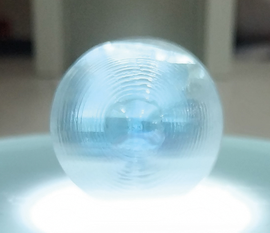
The picture above shows a view, from the bottom, of a crystal of (AlxGa1-x)203 produced by the Czochralski method.
REF
D. Zakgeim et al. Appl. Phys. Express 15 025501 (2022)


