
ST and CNR-IMM researchers win award for 4H-SiC paper
Scientists from ST and the Institute for Microelectronics and Microsystems at the National Research Council of Italy (CNR-IMM) have won the IRPS (IEEE International Reliability Physics Symposium) 2021 best paper award for their research on the relationship between certain defects and the viability of SIC power devices.
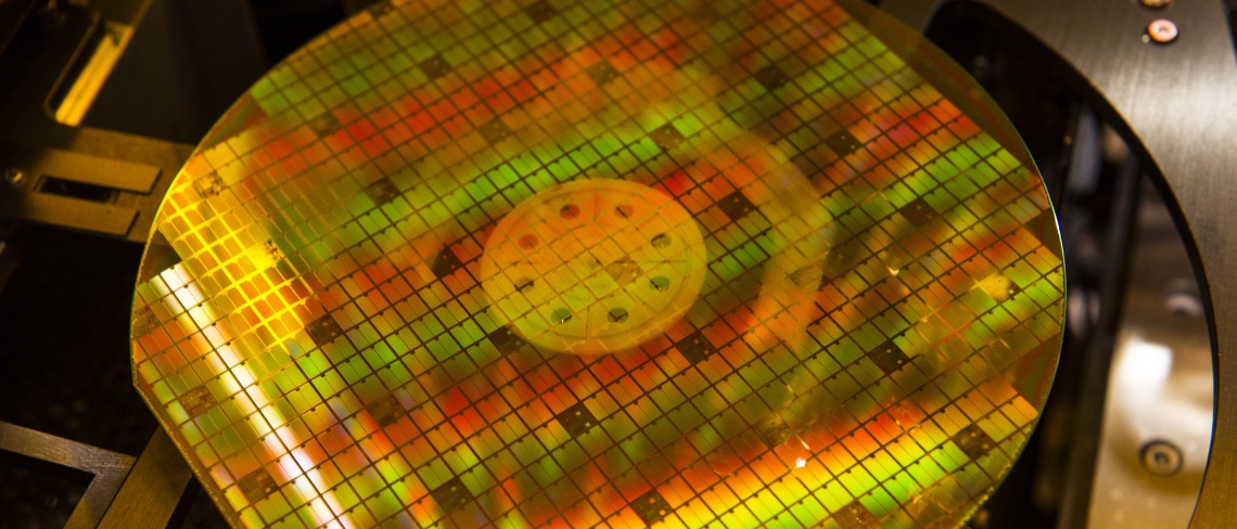
Both teams share a space in ST’s site in Catania, Italy, where they work on SIC and GaN.
The research paper points to two types of defects: short-term and long-term. Among the first, the most severe is the t = 0 type since it’s non-functional from the start. The paper is unique because, for the first time, it exposes a direct relation between crystalline defects and failure rates in t = 0 4H-SiCs. 4H-SiC is a favourite because of its physical characteristics. It offers better electron mobility than 6H-SiC at 947 cm2/Vs but is easier to manufacture than 3C-SiC thanks to its atomic structure of four bilayers in a hexagonal lattice.
The team used atomic force microscopy and cross-sections using scanning electron microscopes to look at t = 0. What they found is the presence of a crystalline precipitate at the bottom of the epitaxial layer that measures about 1.90 µm in height. The authors’ drive to understand why these devices were “dead on arrival” led them to look deeper and discover a new relationship between crystalline precipitates and the rate of defects. Hence, the paper from ST and CNR-IMM received the award because it explored SiC die in a new way.
Since the publication of this paper, ST has learned to optimise the epitaxial reactor chamber and the manufacturing process of 4H-SiC devices to improve yields and make more cost-effective and longer-lasting devices. In turn, ST says it expects 4H-SiC power MOSFETs to penetrate even more markets and applications and thus help increase energy efficiency.
Stress-testing the remaining 4H-SiC Die
Once the researchers winnowed out the t = 0 dice, they put the functioning ones in a package and stress-tested them. The first challenge was a high-temperature gate bias stress, which upped the electric field at the gate oxide. The reason the scientists pushed the devices so hard was to monitor behavior in normal and harsh conditions. Interestingly, they noticed that some of the devices already exhibited abnormal behavior at 3 MV/cm. To understand why it happened, they examined the problematic dies under atomic force microscopy, which revealed the presence of bumps on the gate oxide measuring between 20 nm and 30 nm.
The finding was a breakthrough because it helped sort devices that appeared to work correctly at first but suffered from defects near impossible to spot during production. Not only did the research paper explain why the devices had anomalous gate conduction, but it showed the importance of high-temperature gate bias testing. The results will thus help foundries looking to monitor their SiC devices’ quality better.
High-Temperature Reverse Bias
After the first stress tests, the dice underwent another trial: a high-temperature reverse bias. The benchmark lasted three months and served to simulate decades of normal use. In a nutshell, it helped the authors determine if all the devices would behave normally over their entire lifecycle. And while 98 percent of them did, the other 2 percent revealed abnormalities with gate currents seven times higher than normal. In a real-world application, such behavior would represent a severe malfunction. The challenge is that the defect, coined “silent killer”, while always there, would only manifest after years of normal use.
The authors first used a scanning electron microscope to understand what went wrong but couldn’t perceive anything abnormal. As a result, they switched to transmission electron microscopy, which revealed the presence of a defect in the semiconductor under the gate’s insulator. To further understand what it was, the authors used atomic force microscopy, which enabled them to discover a triangular defect with a height between 18 nm and 30 nm, depending on the stress test’s duration. At this point, they understood that there was a threading dislocation from the substrate to the epitaxial layer. Consequently, they used scanning capacitance microscopy to show the physical impact on the MOSFET device and explain its faulty electrical behavior.
ST says it's only because the scientists used so many investigative techniques that they were able to understand what happened. Put simply, the threading dislocation affects the valence band of the 4H-SiC device, effectively shrinking its bandage.
SiC’s wide bandage is responsible for the device’s excellent electrical properties. Hence, anything responsible for its shrinkage will negatively impact the structure severely. In this instance, the valence band increased by about 0.8 eV to 1 eV, which is significant. Comparatively, SiC has a bandage that varies between 2.3 eV and 3.3 eV, with 4H-SiC sitting at 3.23 eV.
'Correlation between MOSFETs breakdown and 4H-SiC epitaxial defects' by P. Fiorenza et al; 2021 IEEE International Reliability Physics Symposium (IRPS), 2021,


