
Enkris releases Full Color GaN series
Company also expands LED wafer size to 300mm for micro-LED applications
Enkris Semiconductor, a Chinese pure epi-foundry of GaN wafers, has released what it calls its Full Color GaN RGB series of products with wafer size up to 300mm for the micro-display industry.
GaN-on-silicon LEDs show advantages over those grown on other substrates for micro-LED technology in terms of larger wafer size (200mm – 300mm) and better surface quality. Furthermore, taking advantage of state of the art silicon processing in 200mm/300mm fabs, high performance arrays of tiny (5µm2) micro-LED pixels can be fabricated and integrated on silicon CMOS driver with high yield.
Near-eye-displays such as augmented reality (AR) and mixed-reality (MR) devices, require high-efficiency, ultra-fine-pitch (<5µm) red, green and blue pixels integrated on the same material platform. InGaN materials can emit light efficiently covering the entire visible spectral range by adjusting the Indium content. Although high efficiency blue and green InGaN-LEDs have been achieved, it is still very challenging to grow high efficiency red LEDs due to the pronounced strain in the active region and the poor crystalline quality resulting from the large lattice mismatch between InGaN QWs and GaN buffers.

Picture 2: IQE comparison and EL spectra of Full Color GaN® RGB series of products on silicon and sapphire
Enkris Semiconductor says it has successfully overcome these difficulties by using its patented strain engineering and polarisation engineering. By adopting its bandgap tuning technology, Enkris expands its GaN-on-silicon LED epi-wafer product portfolio to Full Color GaN RGB series of products (wavelength: 390~650nm) on 200mm silicon substrates.

Wavelength uniformity is a key factor for micro-LED displays. Enkris says its Full Color GaN RGB series have excellent wavelength uniformity across 200mm whole wafers (picture 3 above). Moreover, GaN-on-silicon blue LED wafers are available up to 300mm and the wavelength is reasonably good with a standard deviation of less than 2nm (picture 4 above).
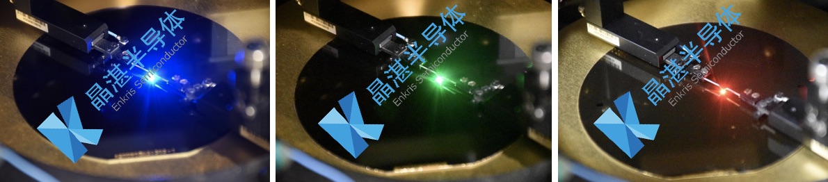
Enkris Semiconductor has also demonstrated RGB micro-LED arrays with pixel size range from 2µm to 50µm, based on its Full Color GaN RGB series of 200mm epi-wafers. Thanks to the high quality epi-wafers, all the pixels can be light up even for each 2µm2 tiny pixel (array: 100 x 100), says the company. This is the key accelerator to the micro-display adoption, according to Enkris.
Kai Cheng, Enkris’ founder and CEO comments: “For monolithic integration of micro-LEDs, it is a critical step to integrate all three colours into a single material platform of large size GaN-on-silicon our Full Color GaN series products will fulfil the industry’s requirement for AR/MR systems. In addition, the GaN-on-silicon wafer size can be scaled up to 300mm and we presented 1200V 300mm GaN-on-silicon platform in September 2021.
"The new platform of 300mm GaN-on-Si LED will show great promise in heterogeneous integration of GaN optical devices, GaN electronic devices and silicondevices. Enkris is now able to supply true RGB GaN-on-Si epitaxial solution for display industry and empower the development of full colour micro-display, and embrace the era of Metaverse.”


