
First integrated laser on lithium niobate chip
Harvard and industry collaboration paves the way for high-powered telecommunication systems
For all the recent advances in integrated lithium niobate photonic circuits — from frequency combs to frequency converters and modulators — one big component has remained frustratingly difficult to integrate: lasers.
Long haul telecommunication networks, data centre optical interconnects, and microwave photonic systems all rely on lasers to generate an optical carrier used in data transmission. In most cases, lasers are stand-alone devices, external to the modulators, making the whole system more expensive and less stable and scalable.
Now, researchers from the Harvard John A. Paulson School of Engineering and Applied Sciences (SEAS) in collaboration with industry partners at Freedom Photonics and HyperLight Corporation, have developed what they believe is the first fully integrated high-power laser on a LiNbO3 chip, paving the way for high-powered telecommunication systems, fully integrated spectrometers, optical remote sensing, and efficient frequency conversion for quantum networks, among other applications.
“Integrated LiNbO3 photonics is a promising platform for the development of high-performance chip-scale optical systems, but getting a laser onto a LiNbO3 chip has proved to be one of the biggest design challenges,” said Marko Loncar, the Tiantsai Lin Professor of Electrical Engineering and Applied Physics at SEAS and senior author of the study. “In this research, we used all the nano-fabrication tricks and techniques learned from previous developments in integrated LiNbO3 photonics to overcome those challenges and achieve the goal of integrating a high-powered laser on a thin-film LiNbO3 platform.”
The research is published in the journal Optica.
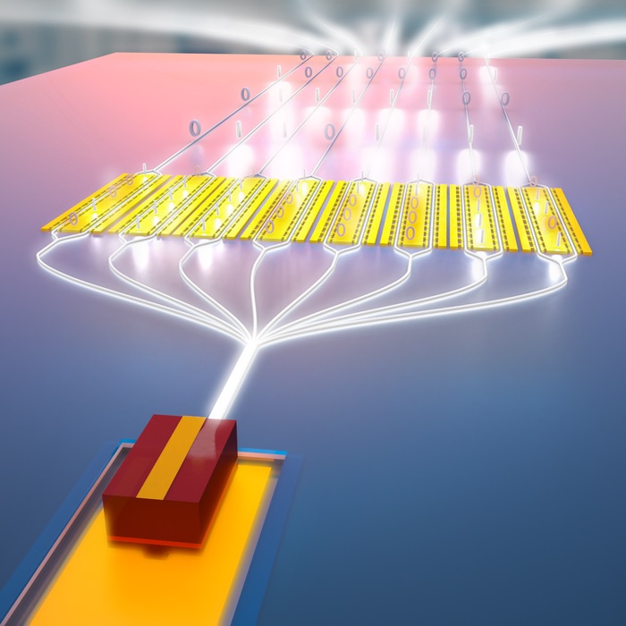
Loncar and his team used small but powerful distributed feedback lasers for their integrated chip. On chip, the lasers sit in small wells or trenches etched into the LiNbO3 and deliver up to 60 milliwatts of optical power in the waveguides fabricated in the same platform. The researchers combined the laser with a 50 gigahertz electro-optic modulator in LiNbO3 to build a high-power transmitter.
“Integrating high-performance plug-and-play lasers would significantly reduce the cost, complexity, and power consumption of future communication systems,” said Amirhassan Shams-Ansari, a graduate student at SEAS and first author of the study. “It’s a building block that can be integrated into larger optical systems for a range of applications, in sensing, lidar, and data telecommunications.”
By combining thin-film LiNbO3 devices with high-power lasers using an industry-friendly process, this research represents a key step towards large-scale, low-cost, and high-performance transmitter arrays and optical networks. Next, the team aims to increase the laser’s power and scalability for even more applications.
Harvard’s Office of Technology Development has protected the intellectual property arising from the Loncar Lab’s innovations in LiNbO3 systems. Loncar is a cofounder of HyperLight Corporation, a startup which was launched to commercialise integrated photonic chips based on certain innovations developed in his lab.
The research was co-authored by Dylan Renaud, Rebecca Cheng, Linbo Shao, Di Zhu, and Mengjie Yu, from SEAS, Hannah R. Grant, Leif Johansson from Freedom Photonics and Lingyan He and Mian Zhang from HyperLight Corporation. It was supported by the Defense Advanced Research Projects Agency under grant HR0011-20-C-0137 and the Air Force Office of Scientific Research under grant FA9550-19-1-0376.
'Electrically pumped laser transmitter integrated on thin-film lithium niobate' by Amirhassan Shams-Ansari et al; Optica 9, 408-411 (2022)


