
Flexibility between lab and fab
As epitaxial structures become more complex, quality control adopts lab methods.
BY TIM GORTER AND LARS GRIEGER, MALVERN PANALYTICAL
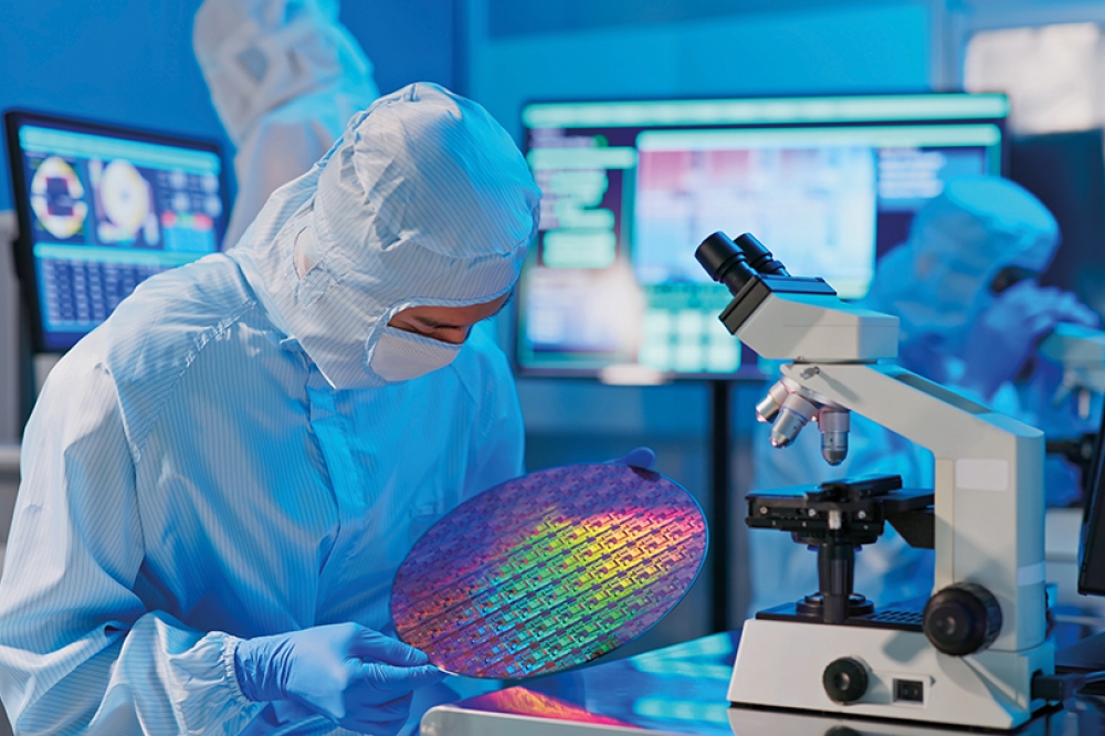
COMPOUND SEMICONDUCTOR functionality is all about the layer structure. But unlike a cake, it’s rare that you wish to slice up your wafer to see what is going on inside.
Fortunately, though, in this instance you can turn to metrology technologies, such as X-ray diffractometry (XRD), to generate accurate and precise structural metrology in a non-destructive manner. Here, advanced capabilities beyond the rocking curves are becoming ever more important for the production of epitaxial wafers.
Production of compound semiconductor wafers continues to rise, as our society seeks to unlock the potential of these materials that offer significant sustainability benefits. If you are a regular reader of this magazine, you will know all too well about the energy savings that come from widespread deployment of compound semiconductors in LEDs or power converters. Increasing manufacturing excellence of compound semiconductor lowers cost, so that these chips can feature in even more electronic products shipped and sold around the globe. The epitaxial growth these devices is monitored by XRD techniques – but what does the maturation of the compound semiconductor industry mean for analytical XRD instruments and those who use them?

The infrastructure for metrology tools located at R&D sites are different compared to fabrication sites
Method transfer from lab to fab
A significant difference between a typical fab and the majority of research labs is the performance criteria for the equipment. Often the difference comes from the jump in the accompanying quality benchmarks that must be met. Almost all CS fabs maintain a cleanroom environment in line with ISO and federal classifications for their epitaxial department. Consequently, fabs need to adopt the latest Semiconductor Equipment and Manufacturing International (SEMI) standards to ensure that production lines comply with ISO cleanroom practices and enable their yield targets.
In parallel, automation is increasingly widespread, justified by the grown volume in these markets. It is a valuable asset in semiconductor production, with automated solutions reducing the need for human involvement and cutting contamination.
Of course, a significant upfront investment may be needed to set up a fab with the appropriate instruments, technologies, and quality controls to ensure that it runs smoothly – and the financial outlay can cause headaches of its own.

By making machines futureproof and flexible, Malvern Panalytical keeps
working ahead of customer needs and developments within the market,
building on years of experience.
The good news is that solutions exist to spread the CapEx. As a compound semiconductor company matures, its needs to undergo a development process, evolving from lab procedures to fab processes. But with multiple options available to those responsible for the tool portfolio employed for the chip production process, making the right choice would appear to be a critical, tough challenge. How does one decide which tool will provide the best functionality and support to ensure a smooth scale-up from research to production? And how can one make sure it is delivered in time?
The MRD XL consists of a base module containing the measurement chamber
and a frontend providing the automation capability. This makes lab
functionality like in-plane measurements available on the fab floor,
integrated into standard receipes.
At Malvern Panalytical, we understand what makers of compound semiconductor epiwafers and devices are looking for in their XRD solutions. It all starts with advanced, accurate, precise characterisation of the structural composition of epitaxial wafers – in fact, it all starts with our X’Pert3 MRD XL. Flexible and reliable, the MRD XL is a world leader in X-ray scattering applications for semiconductor industries.
Drawing on four decades of experience in this arena, our technology remains at the cutting edge of what is possible – but wherever our customers are in their own journey, from development to production, we pride ourselves on having the systems that will support them every step of the way.
Our goal is to ensure that our high-performance instruments and software programs are accessible to labs and fabs working at all stages of the process, from research to quality control. In line with this, our MRD XL is a fully modular design.
By adopting this approach, companies may begin by purchasing our core machine for R&D, before buying add-on fab components from us as and when their operations require them to. It’s an approach that avoids a huge initial outlay for a ‘fixed’ solution that provides functionality beyond what is initially needed. When XRD techniques or production requirements change – by becoming more automated, for example – we recommend purchasing new hardware and software modules, which are easily integrated with the MRD XL.
Having a metrology tool with the flexibility to keep pace with the growth of a product and its manufacturer is a major asset. This is true for small and medium enterprises, for niche fabs producing several different product lines on a single machine and product lines in large fabs that require increasingly complex metrology.
When these firms invest in an MRD XL, it can flex between research to pilot-scale fabrication and finally to full-scale production and back. By growing the capability of the MRD XL piece by piece, fab managers have far more flexibility when considering their CapEx budgets and timeframes.

It is labour intensive to manually place wafers into metrology equipment and less reproducible than a robot with prealigner
Automation is obviously a significant factor in realising the desired cleanroom status. As robotic capabilities continue to advance – perhaps as far as ‘lights-out’ fabs with no hands-on human interference – the importance of relevant SEMI standards is sure to rise. There will be more requirements to adhere to, such as the SEMI E5 (SECS-II) and E30 (GEM) standards, a pair of key protocols governing communications between the equipment and the host or carrier. Enabling the transfer of bespoke measurement data, these interfaces are essential to the success of any semiconductor fab infrastructure.
Delivering superior semiconductor materials and devices clearly depends on much more than just having excellent XRD metrology for wafer analysis. SEMI-standard fabs have to have a consistent, high-quality, reliable process for chemical mechanical polishing (CMP), both for substrate polishing and during processing. Just as a layered cake may need its top trimmed and flattened before icing is applied, a wafer surface needs the right planarity to ensure that all the deposited layers sit on top of one another exactly as required. Here our particle sizing products Mastersizer and Zetasizer allow tight control of slurry specs with a push of a button.
In any fast-moving industry, decision makers must keep an eye on the future – or find a trusted partner with the capabilities to do that for them. For those chip makers and developers partnering with us, this is not a concern for them, because they never need to worry about investing in lab-to-fab equipment that will quickly be outstripped by newer models. Our solutions are informed by decades of experience, a wealth of expertise and run easily for more than a decade.

Malvern Panalytical delivers a multitude of metrology tools for the
semiconductor and electronics industry such as particle characterization
equipment used for CMP slurries, like the Mastersizer
Some compound semiconductor developments are already coming into view on the horizon, such as lights-out fabs, the shift to larger wafer sizes, and the increasing complexity of superlattices in compound semiconductors. Other, more distant advances are harder to foresee. But we are dedicated to continuously improving and upgrading our hardware and software to ensure that these solutions – and our customers – are always ready to tackle and overcome the next challenge.
Malvern Panalytical understands the full process from front-end to electronics assembly and offers more solutions, not mentioned here


