
Simplifying displays with porous GaN microLEDs
GaN-based red microLEDs are now delivering a comparable performance to
their blue and green cousins, thanks to the introduction of a simple
step that produces porous material
BY TONGTONG ZHU FROM POROTECH
OVER OUR LIFETIME displays are continuing to evolve. Many of us have already witnessed a shift from TVs based on cathode ray tubes to those featuring liquid crystals, initially backlit with cold cathode fluorescents and now LEDs. Over the coming years, we shall see a growth in sales of near-eye displays, supporting virtual reality, head-up displays and augmented/mixed reality applications.
These emerging forms of technology are placing tougher demands on display performance. Driven by this demand, new display technologies are undergoing rapid development, with microLEDs leading the way. These miniature marvels are the front runner for next-generation displays, because compared with rival technologies based on LCDs, LEDs, miniLEDs and organic LEDs, they offer an outstanding set of attributes: superior brightness, high contrast, unparalleled efficiencies, a longer lifetime, and increased stability. What’s more, thanks to the ‘micron-scale’ size of these microLEDs, they deliver a far higher image resolution.

Figure 1. (a) Porotech employs a relatively straightforward set-up for
electrochemical etching. The inset shows a photograph of a sample after
etching under room-light illumination. (b) Schematic of the DBR
structure. (c) Cross-sectional scanning electron microscopy image of
the 10 pair GaN/mesoporous-GaN DBR structure.
To match human visual receptors and provide a really realistic image, full-colour displays need to combine sources with red, green and blue emission. This requirement has led designers to employ red, green and blue emitters that can be independently modulated. Ideally, this is accomplished with a simple, lightweight display architecture that is capable of meeting all criteria for next-generation displays.
In such an architecture, it is the norm to employ InGaN-based microLEDs as the high-efficiency blue and green emitters. With conventional means, it is not possible to stretch the emission of these devices to the red while retaining efficiency, so the source that’s used to cover that spectral domain is the red AlInGaP microLED. Combining this with InGaN devices emitting in the blue and green offers a way to make full-colour displays.
Unfortunately, this mixed-material approach is far from ideal, presenting several significant barriers to widespread adoption of microLED-based displays. One concern is that compared with InGaN-based devices, red AlInGaP LEDs suffer from a more severe drop in efficiency as device size diminishes. This makes it difficult to meet the performance and pixel sizes demanded by the likes of alternative-reality and mixed-reality applications. Another concern that’s also related to the performance of the AlInGaP LED is that its decline in efficiency with increasing temperature is far more pronounced than that for its GaN-based cousin, adding complication and expense to the final display design.
As well as those stumbling blocks associated with performance-related criteria, there are issues related to production costs. Mixing multiple material systems over micron-length scales necessitates the development of complex and expensive mass-transfer technologies for positioning individual red, green and blue chips into the desired pixel design. One consequence is a substantial addition to the final device cost, limiting applicability of this approach to the mass market.
Removing barriers
To address these issues, our team at Porotech, a spin out of the Cambridge Centre for Gallium Nitride, has developed a porous InGaN platform that delivers all three primary colours with a high efficiency. Realising red emission with InGaN has not been easy, due to strain that stems from the lattice mismatch between InGaN and GaN. This condition limits the proportion of indium that can be incorporated within the InGaN quantum well, and therefore restricts emission to shorter wavelengths. To relieve this strain, we introduce an engineered subsurface porosity. This allows more indium to be incorporated into the wells, and ultimately extends emission into the red.
The benefits of our technology are not limited to the obvious, crucial breakthrough of realising all three colours on the same InGaN platform. Additional strengths of our approach are that they tackle the efficiency-size problem for the red emitter, and they simplify the transfer technology for making full-colour displays. Furthermore, since the porosity we introduce is sub-surface, the surface is left intact – this means that the rest of the supply chain for LED device manufacturing does not require adaption in its processes or investment in new equipment. It is also worth noting that by introducing strain relief, we ensure an additional benefit of reduced wafer bow – this simplifies and increases the yield of monolithic displays produced by direct wafer-to-wafer bonding. And last but by no means least, our process is highly scalable and reproduceable, ensuring excellent uniformity across the wafer, from wafer-to-wafer, and from batch-to-batch.

Figure 2. Atomic force microscopy images of a template surface (a)
before and (b) after electrochemical porosification, showing that the
smooth surface and the epi-ready terraces are maintained. Z-scale
(black to white): 4 nm.
One of the essential building blocks for developing next-generation optoelectronic devices is the distributed Bragg reflector (DBR). Formed from alternating layers of high and low refractive index material, the DBR can be thought of as a one-dimensional photonic crystal. When incorporated within an LED, the DBR acts as an integrated mirror and/or filter, helping to direct and tune the emitted light. As well as providing high reflectivity and low absorption, the DBR ideally has good conductivity, allowing efficient electrical injection of charges into the device. An excellent candidate for the DBR is the non-polar III-nitrides, a family of materials that combine higher rates of radiative recombination for improved device efficiencies with unique, attractive properties, such as the emission of strongly linearly polarised light. Note that non-polar DBRs are used alongside conventional, polar LEDs, making this technology applicable to today’s high-volume fabs.
It is very difficult to apply conventional epitaxy-based polar nitride DBR fabrication, involving the growth of alternate layers of different nitride alloys with different refractive indexes, to non-polar orientations. The problem is that there are no available alloys that will lattice-match to non-polar GaN. Attempts to do so lead to cracking and low reflectance.
Overcoming this issue are a number of DBR fabrication strategies for non-polar GaN-based structures, including mesoporous DBRs. This form of DBR has much merit, offering a spectral response that can be tuned in three ways. As well as adjusting the layer thicknesses and the number of repeat periods – this pair of levers can be applied to all forms of DBR – porosity can be varied, leading to changes in refractive index contrast.
Our core technology is based on the mesoporous DBR, which we have collectively spent decades studying and developing.
We advocate a one-step, selective electrochemical process for porosification (see Figure 1 for an illustration of this process, as well as an image of the resulting DBR microstructures). This step can be carried out at room temperature in constant voltage mode using no UV illumination, with the removal of material monitored via the etching current signal. The electrochemical process begins with localised injection of holes, driven by applying a positive anodic bias. Alternating n+-GaN layers are oxidised under this condition.
A cross-sectional scanning electron microscope image of the resulting nanoporous DBR structure confirms that it is just the n+-GaN layers that are etched into the mesoporous structure (see Figure 1 (a)). Etching is uniformly achieved across the entire sample that’s submerged in the etching solution, demonstrating the high uniformity of the process. When processing batches of wafers in this way, a high level of uniformity is maintained wafer-to-wafer and batch-to-batch – this demonstrates the scalability of this approach and its applicability to mass-manufacture of optoelectronic devices.
One of the major advantages of the selective porosification process is that, by only etching the n+-GaN layers, by design the surface of the template remains unchanged. Evidence of this is provided by atomic force microscopy images of a template before and after electrochemical porosification (see Figure 2). It is possible for etching to penetrate undoped GaN layers via nanoscale vertical pathways that exist in the as-grown material (no pre-patterning is necessary).
A practical implication of maintaining the same surface is that the porous wafers can be processed into LEDs without having to change any downstream processes. Or, to put it another way, chipmakers can exploit the benefits of the porous DBR structures without having to disrupt their device manufacturing supply chain.
Device demonstrations
We have shown that porous GaN templates can be processed into LEDs using industry-standard recipes, and that the resulting devices deliver an improved efficiency, thanks to the mesoporous DBR structure.
Our initial demonstration involved the use of MOCVD for GaN template growth and LED regrowth. We grew a pair of templates with a dislocation density of around just 3-6 x 108 cm-2 and a latent mesoporous-DBR structure, formed from alternating layers of undoped and highly n-doped GaN. We applied an electrochemical porosification process to one of the wafers, before processing both into blue-emitting p-i-n LED structures (see Figure 3 (a) for an illustration of the device’s design, and (b) and (c) for optical micrographs, demonstrating the relatively uniform electroluminescence emission from both non-porous and porous samples). As the uniformity of emission is similar in both structures, we can conclude that the growth of the LED layers is not significantly altered by the presence of the mesoporous-DBR in the regrowth template.

Figure 3. Porotech has processed wafers (a) to produce (b) non-porous LEDs and (c) a mesoporous DBR LEDs.
Electrical and optical measurements have been conducted on both types of LED. Plots of the light output at various drive currents show that the introduction of porosity to the DBR delivers an increase in the maximum efficiency, and shifts the onset of efficiency droop to a higher current density (see Figure 4). In both samples, the shift in peak wavelength with injection current is similar.
By demonstrating a similar performance with increased efficiency, we have equipped our team with the foundation for delivering InGaN-based blue, green and, critically, red microLED technology and products. Another benefit that comes from using the porous structure is a reduction in wafer bow – it is trimmed by more than 30 percent, due the strain relief that stems from the introduction of porosity. Reducing bow helps to ensure a high-yield LED for epiwafer production, chip processing and wafer-to-wafer bonding, especially for microLED displays, where it is crucial to have better than micron-scale precision.

Figure 4. (top) Light-current (L-I) measurements for devices made by
Porotech that are processed on porous and non-porous templates.
(bottom) Plots of peak position showing similar blue-shifts with
increasing injection current.
A red revolution
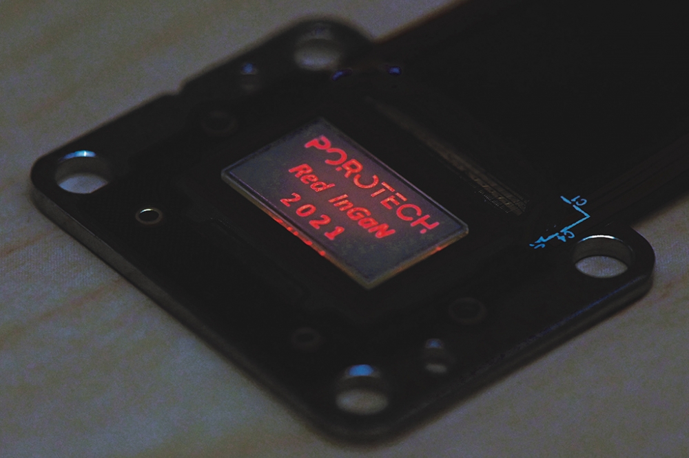
Following further development, we have used our porous platform to deliver the world’s first native InGaN-based red microLED. This milestone removed a key bottleneck for the whole industry. Our porous structure relieves strain that is introduced by the lattice mismatch between the InGaN and GaN, and allows greater concentrations of indium to be incorporated without degrading material quality. Emission is shifted to the red, with the peak wavelength occurring at 640 nm (see Figure 5).

Figure 5. Porotech’s demonstration of the world’s first native red InGaN-based microLED using its platform technology.
We have used our porous-enabled red microLED technology to produce the world’s first native InGaN-based red microdisplay (see Figure 6), which has an active area of 0.55 inches diagonally and a resolution of 960 by 540, equating to 2000 ppi. This microdisplay provides an initial and quick demonstration that proves the capability of our technology. When we remove sapphire, we expect an increase of the brightness of this display and reduced backscattering.
With this demonstration we have shown, for the first time, that all three light-emitting elements can be produced with a single toolchain. This breakthrough highlights how to eliminate the complexity and expense associated with fabricating displays that mix devices from different material families.

Figure 6. Porotech has demonstrated the world’s first native InGaN red
micro-LED display. Note that the sapphire has not been removed – hence
further improvements in backscattering and brightness can be achieved
with further optimisation
Our successes have placed us in an enviable position where we can play a crucial role in the future of microLED displays. We are attracting much attention, thanks to our demonstration of the world’s first native InGaN red microdisplay, and the breaking of a major barrier, by showing that a single material system can be used to make green, blue and red microLEDs. The scalability of our process, along with the lack of disruption to the rest of the supply chain, positions our technology as a critical enabler for the mass manufacture of next-generation display technologies.


