

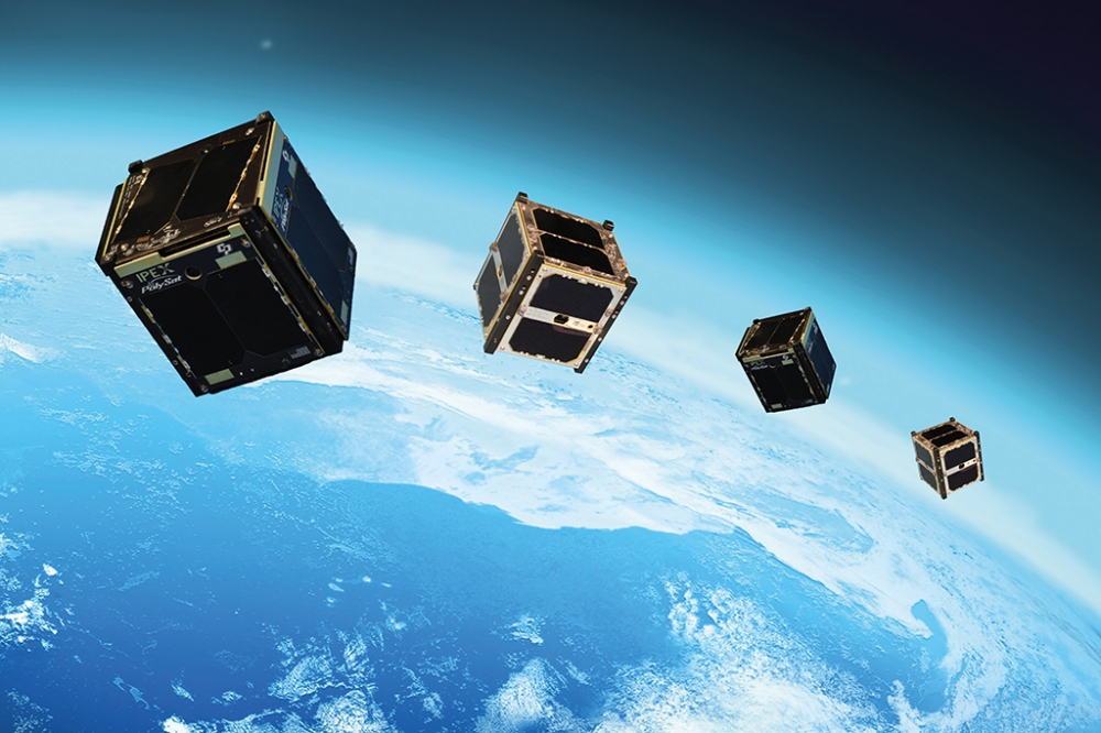
Getting PICs off the ground
PICs based on InP and GaAs prepare to slash the size, weight and power
of systems to be deployed in space and on-board aircraft for a variety
of sensing applications
BY JONATHAN KLAMKIN, PAUL VERRINDER, VICTORIA ROSBOROUGH AND FENGQIAO SANG FROM THE UNIVERSITY OF CALIFORNIA SANTA BARBARA
ONE OF THE MOST powerful technologies of our time is the photonic integrated circuit (PIC). By integrating all the required functions on a single chip, the PIC significantly reduces the cost, size, and weight at the system level, while improving performance, stability, and reliability.
To produce this multi-faceted photonic device, wafers are processed in a manner that is similar to that employed for the electronic circuits that have revolutionised our society. However, the materials that are used can be somewhat different. While silicon is the semiconductor of choice for making electronic circuits, those employing photonics can also be formed from InP and GaAs. Both these III-Vs are attractive options, because they enable monolithic integration of gain material for light sources and their amplification.
Pioneers of the PIC developed this technology with telecommunications applications in mind. They focused on the centre-band, or C-band, which spans the spectral range from 1530 nm to 1565 nm, a domain associated with ultra-low-loss transmission of light through an optical fibre. Recently, though, PICs have gained traction in applications involving the O-band (1260 nm to 1360 nm), such as optical interconnects within and between data centres.
Note, though, that the potential for PICs is not limited to these wavelengths, nor to communications, or even to terrestrial applications. There are opportunities lying well beyond these boundaries, such as those we are exploring at the University of California, Santa Barbara (UCSB). We are targeting space and airborne applications of PICs, namely free-space communications, remote lidar for gas sensing and topographical lidar. Our work on free-space communications has focused on extending the power-handling capabilities of InP PICs. Success on this front opens the door to higher data rates and/or longer link distances. Output powers with our InP PIC platform have exceeded 250 mW, a value far higher than any previous demonstration.
We have also broken new ground while participating in a NASA-funded project entitled IMPRESS Lidar – short for Integrated Micro-Photonics for Remote Earth Science Sensing Lidar. Through this project we have demonstrated the first ever fully functional PIC-based gas remote sensing lidar system that targets atmospheric CO2. This system operates near a relatively weak absorption line that is centred at 1572.335 nm, a wavelength falling within the communications L-band (1565-1625 nm) that allows us to leverage mature InP PIC technology. Through this project we have been able to demonstrate a shrinking of the system volume by a factor of more than one hundred, compared with a system built with discrete components by collaborators at NASA.
Another avenue explored by our team has been the development of a GaAs-based PIC, which extends operation to other spectral domains. This tuneable laser PIC, developed for 10XX nm wavelengths, features beam-steering capability when it is used in conjunction with diffractive optical elements.

Figure 1. Overview of III-V PIC fabrication process
Sensing gases with InP PICs
Our InP PIC platform, equipped with high-efficiency lasers, provides broad wavelength coverage across the 1.2 µm to 1.6 µm range. This platform is ideal for active remote sensing of CO2, which can be accomplished with a laser source at the sensing wavelength of 1572.335 nm, using a sensing window of 30 GHz. A PIC-based approach for CO2 sensing has many merits over the active remote sensing systems formed from commercial off-the-shelf optical components, which are compromised by their size, weight, and high power consumption. Usually, sensing experiments are performed from a near earth orbit, to minimise the high cost associated with launching large spacecraft into orbit. One of the strengths of our PIC technology, which has the potential to enable systems that are far more compact and power efficient, is that it could lead to increased deployment of this form of sensor on small spacecraft that launch more often.

Figure 2. (a) Simplified side-view schematic of an offset quantum-well
PIC platform. Scanning electron microscopy images of (b) the top-view of
fabricated gratings for the sampled grating distributed Bragg reflector
(SGDBR) lasers, (c) cross-section of a fabricated ridge waveguide, (d)
plan-view of two parallel waveguides, and (e) plan-view of a directional
coupler with a 1 µm gap between the waveguides. (f) Top-view optical
microscope image of a fully fabricated CO2 lidar PIC.
The PICs we produce are designed and fabricated with what we refer to as an offset quantum-well platform. We deposit multi-quantum wells on top of a low-loss waveguide core in such a way that the wells are slightly offset from the centre of the vertical optical mode. Taking this approach enables us to selectively remove the wells to form separate active and passive regions. Coupling between those regions is high, typically between 90 and 95 percent, with reflections managed by angled interfaces. The active regions, where wells remain, provide gain in laser cavities and optical amplifiers. Meanwhile, the passive regions, where wells are absent, contain mirrors, filters, phase-tuning elements and optical modulators, as well as interconnects between sections and components (see Figure 2(a) for a sideview of the offset quantum well PIC platform used for InP CO2 active sensor development).
To form our gratings, we etch into the waveguide core layer after defining active and passive regions. Adopting this approach enables us to form sampled grating distributed-Bragg-reflector (SGDBR) lasers, which provide leader and follower lasers for the active sensor. These lasers combine a gain section for generating photons with a back SGDBR mirror, a front SGDBR mirror, and a phase tuning section. As the sections of the laser are electrically isolated, each can be addressed separately. In addition to providing gain for a laser, active sections may also be used to form: a photodiode, which operates under reverse bias; and a semiconductor optical amplifier, operating under current injection. The amplifier can compensate for passive waveguide losses and boost the PIC output power.
Images acquired with a scanning electron microscope reveal the various elements during the fabrication process (see Figure 2 (b) to (e)). Even with an optical microscope, it is possible to identify the various components of a PIC designed to sense CO2 using lidar. This PIC, with a footprint of approximately 0.8 mm by 8.3 mm, employs passive waveguides and directional couplers to route optical signals and connect active and passive elements. After the leader laser is a directional coupler and a phase modulator, the latter of which stabilizes the laser. The follower laser is followed by a directional coupler and a semiconductor optical amplifier, incorporating a high-speed pad configuration that enables encoding of high extinction pulses. Directional couplers tap a fraction of the signals from the leader and follower lasers, routing the combination to a high-speed photodiode.

Figure 3. PIC remote lidar CO2 sensing architecture and test schematic.
Our PIC-based CO2 sensing architecture, illustrated in Figure 3, features a leader laser that is locked to the 1572.335 nm CO2 absorption line by an absolute CO2 reference cell. An integrated phase modulator, driven at 125 MHz, enables the use of a frequency modulation technique. Fed with an output signal, a mixer extracts an error signal, which is fed to a control servo for signal filtering and processing, and coupled to the phase section of the leader laser to realise locking. An optical phase-lock loop, leveraging the high-speed photodetector for beat-note detection, enables the follower laser to be offset-locked to the leader laser by +/- 15 GHz. The output of the follower laser is coupled to a semiconductor optical amplifier pulse carver, which aids generation of the desired frequency-stepped pulse train for gas sampling.
An illustration of the measured error signal and gas transmission for the absolute reference cell, measured using the leader laser, is shown in Figure 4 (a). We have measured stabilization over 30 minutes with a 1 second gate time, and compared performance with and without feedback to characterize the relative impact of the stabilization circuit (see Figure 4 (b)). Without feedback, the peak-to-peak frequency stability is typically 675 MHz and the frequency standard deviation 86 MHz. Introducing feedback delivers a tremendous impact, with measurements revealing a reduction in the peak-to-peak stability to 2.75 MHz and a fall in the standard deviation to 465 kHz.

Figure 4. (a) CO2 reference cell absorption and the
frequency-discriminating error signal used to stabilize the leader
laser. The reference is a tube pressurized with CO2. (b) Beat-note
between the leader laser and an external cavity laser with and without
feedback to the leader laser phase section. (c) Beat-note between the
leader and follower laser with and without an optical phase lock loop
(OPLL) engaged. (d) Overlaid spectra measured from the leader and
follower laser as the follower laser is tuned from 1-15 GHz offset. (e)
Exemplary 1 µs pulse generated by sweeping the bias on the semiconductor
optical amplifier from 0 mA to 100 mA. The pulse rise time is 262 ns
and the fall time is 169 ns. (f) Measured absorption of a CO2 test cell
along with a Lorentzian fit. The full-width at half-maximum (FWHM) of
the fit is 1.6 GHz.
Once the leader is stabilized, the follower laser can be offset-locked to it. Our measurements, considering laser stability over 30 minutes with a 1 second gate time, show that the introduction of an optical phase-lock loop cuts the peak-to-peak frequency stability down from 1.36 GHz to 29 kHz, and the standard deviation from 181 MHz to 3.61 kHz.
Additional measurements of this PIC by our team show: that the optical spectra for the stabilized leader laser and for the follower laser can be offset by between 1-15 GHz (see Figure 4(d)); and an exemplary pulse can be generated with the semiconductor optical amplifier that follows the leader laser, demonstrating an extinction of 40 dB when swinging the drive current from 0-100 mA (see Figure 4(e)). We have also generated a frequency-stepped pulse train, enabling measurements of a CO2 sample in a separate pressurized tube cell (results are reported in Figure 4(f)). Taken together, our set of measurements confirm the full operation of our PIC CO2 lidar system.
Topographical lidar with GaAs PICs
As today’s airborne topographical lidar systems tend to be built from commercial off-the-shelf components, such as bulk and discrete optics, this restricts their deployment to larger spacecraft or aircraft. One such example is NASA’s Land, Vegetation and Ice Sensor, which is mounted on a Beechcraft B200 King Air. It will now come as no surprise that to enable deployment on small satellites, such CubeSats, there needs to be a substantial reduction in size, weight and power – requirements that can be realised once again by turning to PIC technology.
For topographical lidar, the laser typically has a wavelength near 1000 nm, which is within a spectral range that has a relatively low atmospheric absorption and benefits from the existence of highly sensitive detectors. As this wavelength region requires the GaAs material platform, we have adapted our PIC platform for this III-V. We have fabricated a widely tunable laser, producing a centre wavelength near 1030 nm, which can be combined with diffractive optical elements for beam steering. Tuning the wavelength of the laser alters the angle of reflection from the grating element and effectively steers the beam, enabling wider surface coverage.
Our laser consists of a gain section, front and back mirrors for coarse wavelength tuning, and a phase section for fine wavelength tuning (see Figure 5 (a) for a side-view schematic, Figure 5 (b) for a top-view microscope image of the fabricated chip, and Figure 5 (c) for scanning electron microscopy image of a laser chip mounted on a carrier, with the metal pads wire-bonded to the carrier traces).

Figure 5. (a) Side-view schematic of GaAs-based widely tuneable laser,
(b) top-view optical microscope image of a fabricated laser, and (c)
top-view scanning electron microscopy image of mounted and wire-bonded
laser chip.
To tune the laser’s output wavelength, we apply a current to the mirror and the phase sections. Coarse wavelength tuning is accomplished by tuning front and back mirrors, while fine tuning is realised with adjustment to the phase section. Our measurements show eight different lasing output spectra overlaid, demonstrating approximately 22 nm of coarse wavelength tuning (see Figure 6 (a)), and the use of the phase section for finer wavelength tuning (see Figure 6 (b)). We have also produced contour plots, which show the laser wavelength as a function of front and back mirror tuning, and demonstrate the full tuning capability (see Figure 6 (c)).
We have also investigated the capability of a semiconductor optical amplifier to increase the output power produced by the PIC (see Figure 6 (d)). For a conventional laser, without a semiconductor optical amplifier, output power is just above 35 mW at a drive current of 100 mA. For that drive current, when an equivalent laser is combined with a semiconductor optical amplifier biased at 100 mA, total output power exceeds 75 mW (see the red curve in Figure 6 (d)).

Figure 6.(a) Overlaid spectra illustrating a 22 nm tuning range, (b)
fine wavelength tuning with phase section, (c) contour plot showing
wavelength as a function of front and back mirror currents, and (d)
power output as a function of current with and without amplification.
Our two PIC platforms developed for space and airborne lidar – the InP PIC platform for active sensing of atmospheric CO2 and the GaAs PIC platform for topographical lidar – highlight the promise of this technology for slashing the size, weight and power of systems serving these applications. Armed with these merits, these systems should see an increased frequency of deployment on small space platforms. To further this, in the near term we shall deliver hardware to our collaborators at NASA, so that they can perform their own sensing experiments in a laboratory setting. In conjunction, we will direct efforts at realising closer electronics integration, as this could lead to even lighter, smaller and more frugal systems. Beyond this, our plans include undertaking some space qualification, such as radiation testing, through ongoing collaborations, and working with NASA to bring our technology to the next level of technology readiness – this is considered an ‘instrument programme’.
The authors acknowledge funding support from NASA, technical contributions from Joseph Fridlander, Shannon Lee, Mark Stephen, Jeffrey Chen, Kenji Numata, Stephan Kawa, Fabrizio Gambini, Guangning Yang, Michael Krainak and Larry Coldren, and technical discussions with Parminder Ghuman and Amber Emory.
FURTHER READING
H. Zhao et al. “High-Power Indium Phosphide Photonic Integrated Circuits,” IEEE J. Sel. Top. Quantum Electron. 25 1 (2019)
H. Zhao et al. “High Power Indium Phosphide Photonic Integrated Circuit Platform” 2019 Device Research Conference (DRC)
J. Fridlander et al. “Dual Laser Indium Phosphide Photonic Integrated Circuit for Integrated Path Differential Absorption Lidar” IEEE J. Sel. Top. Quantum Electron. 28 6100208 (2022)
F. Sang et al. “Integrated Photonics Technology for Earth Science Remote-Sensing Lidar” 2021 IEEE International Geoscience and Remote Sensing Symposium IGARSS (2021)
V. Rosborough et al. “Monolithic Integration of Widely-Tunable DBR and DFB Lasers with One-Step Grating Formation,” in OSA Advanced Photonics Congress (2019)
P. Verrinder et al. “Gallium Arsenide Photonic Integrated Circuit Platform for Tunable Laser Applications” IEEE J. Sel. Top. Quantum Electron. 28 5 (2022)
P. Verrinder et al. “SGDBR tunable laser on gallium arsenide for 1030 nm lidar applications,” 2021 27th International Semiconductor Laser Conference (ISLC), 2021.
J. B. Abshire et al. “Measuring atmospheric CO2 for the NASA ascends mission: The CO2 laser sounder approach” IEEE International Geoscience and Remote Sensing Symposium (2012)


