
Penn State to lead $7.5 Million study of radiation effects on GaN
Interdisciplinary team aims to predict and mitigate radiation-induced damage of wide bandgap semiconductors
To better predict and mitigate radiation-induced damage of wide bandgap semiconductors, the US Department of Defense has awarded a team led by Penn State, a five-year, $7.5 million Defense Multidisciplinary University Research Initiative Award.
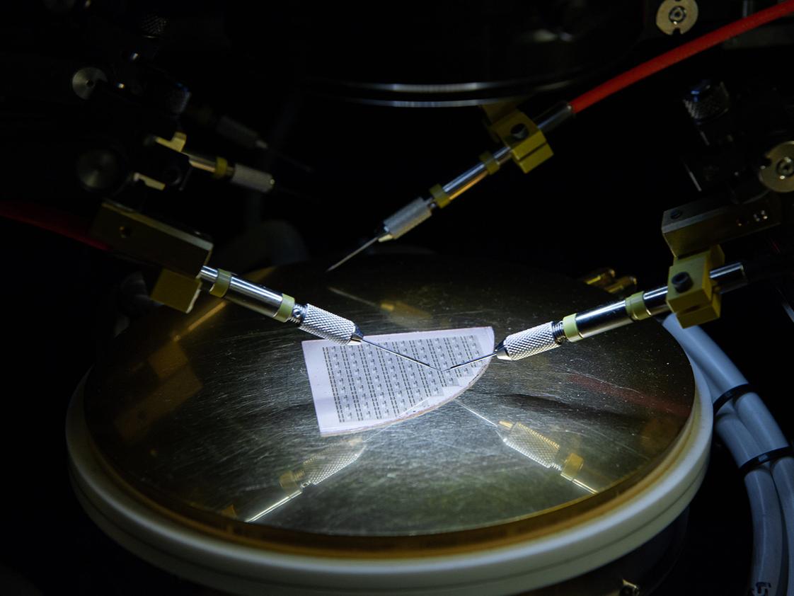
According to Rongming Chu who will spearhead the project, wide bandgap semiconductors, such as GaN, are inherently more resistant to radiation due to stronger atomic bonds, however, researchers have yet to reach the full potential of radiation hardness in wide bandgap semiconductor electronics.
“Preliminary studies have indicated that the radiation resistance appears to be limited by defects in the semiconductors, rather than by the material’s intrinsic properties,” Chu said. “In this project, we seek to understand the radiation effects of these defects so that we may develop a strategy to redesign the wide bandgap semiconductor device for the ultimate radiation hardness.”
Examples of defects include unwanted impurities, displacement of atoms from their original sites and dangling atomic bonds at the interface between dissimilar materials.
“There is a risk of these defects becoming electrically active under a high electric field, with energetic electrons, causing detrimental effects to device performance,” Chu said. “Today’s wide bandgap semiconductor electronic devices are designed such that this risk is minimised under normal operating conditions. However, radiation can force the device out of its normal operating condition by exciting additional energetic electrons interacting with the pre-existing defects. It can also knock atoms out of their original positions, modifying pre-existing defects and generating new defects.”
The project will have an interdisciplinary team. Collaborators include Patrick M. Lenahan, distinguished professor of engineering science and mechanics; Miaomiao Jin, assistant professor of nuclear engineering; and Blair R. Tuttle, associate professor of physics, all from Penn State; and Tania Roy, University of Central Florida; B. Reeja Jayan, Carnegie Mellon University, and Michael E. Flatté, University of Iowa.
Chu noted that, at Penn State, the team will use tools and experts affiliated with the Radiation Science and Engineering Center and the Nanofabrication and Materials Characterisation User Facilities at the Materials Research Institute.
“The strength of our project comes from a combination of expertise: my research group’s capabilities on GaN devices, Lenahan’s expertise in defect spectroscopy, Jin’s radiation damage modeling, Tuttle’s defect theory work, Roy’s electrical characterisation of radiation effects, Jayan’s defect structure characterisation and Flatté’s transport theory work,” Chu said. “The teamwork also extends beyond the investigators of this MURI project — especially Michael Lanagan, professor of engineering science and mechanics, who was very instrumental in coordinating this multidisciplinary team effort.”
The grant will support 16 graduate students, including 11 at Penn State, to perform multidisciplinary research encompassing physics, computation, materials science and engineering and electrical engineering as they pursue a variety of master’s degrees and doctorates.
“Not only will the research prepare next-generation technologists to take on technical challenges, but, through our collaborative work with national laboratories and industry stakeholders, the students will also learn the professional skills needed bridge fundamental research to real-world applications,” Chu said.


