
Improving GaN-on-silicon RF devices
Dialling back the trimethylaluminum flow prior to buffer growth yields high-quality GaN-on-silicon devices with a low RF loss
A team from China and Japan is helping to close the gap in performance between GaN RF devices grown silicon and those formed on SiC, which are superior but more expensive.
Spokesman for the collaboration, Xuelin Yang from Peking University, says that the team’s GaN-on-silicon growth process yields epiwafers that break new ground for dislocation density, while ensuring a low RF loss.
Success on both these fronts has come from tackling issues associated with the growth of the AlN buffer layer. Prior to and during its growth, aluminium diffuses into the silicon substrate, where it acts as a shallow acceptor impurity, forming a p-type parasitic layer that causes RF loss. Yang and co-workers have minimised this diffusion by optimising the trimethylaluminium flow rate.
Note that these researchers are by no means the first to try and improve the quality of GaN-on-silicon material for RF applications by supressing the diffusion of aluminium. Others have turned to either a reduction in growth temperature, insertion of a 3C-SiC blocking layer, substrate nitridation or the use of MBE. While these approaches have suppressed aluminium diffusion and consequently RF loss, this has come at the expense of degradation to crystal quality.
Avoiding this compromise, the team – from Peking University, China’s CEC Compound Semiconductor, the Collaborative Innovation Centre of Quantum Matter in Beijing, and Japan’s International Centre for Materials Nanoarchitectonics – has triumphed by investigating samples produced with a variety of growth and pre-growth conditions.
These trials began by loading 150 mm high-resistivity silicon substrates into a planetary MOCVD reactor and annealing them under hydrogen gas for 10 minutes. Samples were formed by flowing trimethylaluminium for 3 minutes at rates of either 15 sccm, 10 sccm or 5 sccm, prior to the growth of a 90 nm-thick AlN buffer. The team also produced a fourth sample using a pre-flow rate of 10 sccm for 3 minutes, followed by the growth of a 190 nm-thick buffer. For all four samples, the researchers added a 1.3 µm-thick GaN layer, using a lattice-mismatch-induced stress-control technology.
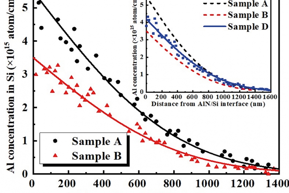
Transmission electron microscopy revealed that the lowest trimethylaluminum flow rate of 5 sccm led to cracks in the epiwafer. With higher flow rates, cracks were absent. Investigating the crack-free samples with secondary ion mass spectrometry (SIMS) showed that dialling back the trimethylaluminium flow prior to AlN growth from 15 sccm to 10 sccm cut the concentration of aluminium at the AlN-silicon interface from 5.5 x 1015 cm-3 to 3.5 x 1015 cm-3. The extent of this reduction followed the fall in trimethylaluminum flow. Measurements also revealed that increasing the AlN buffer thickness from 90 nm to 170 nm increased the aluminium impurity concentration at the substrate surface from 1.8 x 1011 cm-2 to 2.4 x 1011 cm-2.
(Pictured above: For the growth of high-quality GaN layers, the lowest level of aluminium in a silicon substrate comes from a pre-growth flow of 10 sccm, and an AlN thickness of 90 nm (sample B). Sample A had a higher flow of 15 scccm, and sample D had a 10 sccm flow rate and an AlN thickness of 190 nm (sample C, not shown and having a 90 nm-thick AlN layer produced with a 5 sccm flow, had cracks in the epilayers).
Based on the findings provided by SIMS, Yang and colleagues concluded that aluminium diffusion is more sensitive to trimethylaluminum flow prior to AlN growth than the thickness of AlN that is deposited.
To determine RF losses, the team added transmission lines in a coplanar waveguide configuration to their heterostructures. The sample with the lowest level of aluminium diffusion produced the lowest RF loss, of just 0.25 dB mm-1 at 10 GHz. For this sample, the dislocation density is 2.9 x 109 cm-2.
Yang believes that even better results may be possible by investigating a greater range of trimethylaluminum flows and AlN thicknesses.
Reference
C. Ma et al. Appl. Phys. Express 15 031003 (2022)


