
Aixtron delivers deposition tool for advanced research
Boise State University to use MOCVD system for deposition of 2D materials and novel GaN-structures
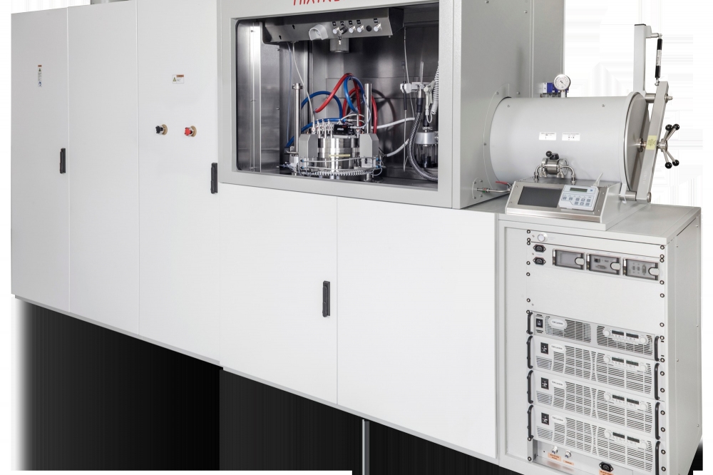
Aixtron will deliver a deposition system from its Close Coupled Showerhead MOCVD product range for compound semiconductor materials to the Boise State University. The CCS 3x2 is part of an infrastructure expansion awarded to Boise State University.
The Aixtron CCS 3x2 has a capacity of 3x2 inch wafers. The system will have a maximum operating temperature of 1400degC which will enable the deposition of graphene and hBN on sapphire as well as novel structures for GaN-based UV LED’s. Equipped with a wide variety of metal-organic and gas channels the system will enable the University to deposit the most advanced 2D materials. In addition, the system includes Aixtron’s proprietary ARGUS and EPISON in-situ metrology technologies which are proven key enablers for the uniform, repeatable wafer scale growth of 2D materials.
With help of the CCS 3x2, Boise State aims to enable up-to-date manufacturing of advanced flexible hybrid electronics using 2D-3D heterostructures. The goal is to use the Aixtron system to research and overcome the challenges of large-scale synthesis and integration of 2D materials into full semiconductor device process flows.
“The Aixtron system is a major part of our research infrastructure expansion. The Aixtron Close Coupled Showerhead MOCVD system is capable of wafer scale growth of atomically thin semiconductor materials as well as more traditional semiconductor films”, says David Estrada, Boise State`s Associate Director for the Center for Advanced Energy Studies and Associate Professor in the Micron School of Materials Science and Engineering.
The Aixtron CCS 3x2 tool is expected to be the only system at a U.S. university dedicated and configured for wafer scale 2D and Nitride-based compound semiconductor growth. It will prepare the future semiconductor workforce at the undergraduate and graduate levels for the U.S. based semiconductor industry.
In close cooperation with Aixtron, the Boise State research team intends to use material properties, AI algorithms and microfabrication techniques to create novel technologies that will drive future applications.
“We are happy to tighten our bonds with the Unites States and the academic world by providing an industrial-grade R&D reactor to Boise State University. Our CCS 3x2 equipment delivers best in class results for 2D-materials at wafer scale in multiple applications. It is also the only system technology that can be configured for combined 2D and GaN research while also allowing the growth of van-der-Waals heterostructures”, explains Michael Heuken, VP Advanced Technologies at Aixtron.


