Loading...
News Article

Sensitron shrinks half-bridge module with EPC GaN FET

News

High power density 350V GaN IPM is 60 percent smaller than alternative silicon solutions

By replacing traditional silicon FETs with EPC’s 350V, EPC2050 GaN FET, Sensitron, a US manufacturer of high rel power electronic components, has been able to reduce the size of its half bridge module by 60 percent while also improving the module’s already junction-to-case thermal conduction.

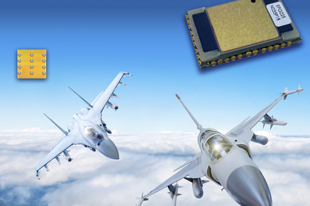
The SPG025N035P1B from Sensitron is a high-power density 350 V, 20 A GaN half bridge with an integrated gate drive, optimised for stray inductance and switching performance at 500 khz. Rated at 20 A, the module can be used to control over 3 kW. Sensitron’s proprietary topside cooling technology on this ultra-small, lightweight high power density package (1.10 inch x 0.70 inch x 0.14 inch) allows for optimal thermal performance. The SPG025N035P1B was designed for commercial, industrial, and aerospace applications.

The SPG025N035P1B module uses the EPC2050, a 350 V rated GaN FET with 80 mΩ maximum RDS(on), 26 A peak current power in a small chip-scale package that measures 95 mm x 1.95 mm. The EPC2050 provides Sensitron with a high efficiency solution due to the low switching losses, and a high-power density solution due to the extremely small size. The EPC2050 is also ideal for multi-level converters, EV charging, solar power inverters, lidar, and LED lighting.

“We are delighted to be working with EPC. By using the ultra-small EPC2050 GaN FET, we could design a 350V half bridge module with higher efficiency and 1/3rd the size of alternative silicon solutions allowing us to capture very high-density applications”, commented Richard Locarni, Director of New Business Development, Sensitron.

Alex Lidow, EPC’s CEO added, “This application is a great example of the real benefits that GaN brings. We have worked closely with Sensitron to find the best GaN FET to meet the design challenges that the power-density requirements of their module demands.”

QD company Quantum Science expands into new facility
Innoscience files lawsuit against Infineon
Riber revenues up 5% to €41.2m
Forvia Hella to use CoolSiC for next generation charging
Photon Design to exhibit QD simulation tool
Ortel transfers CW laser fabrication to Canada
Luminus adds red and blue multi-mode Lasers
PseudolithIC raises $6M for heterogeneous chiplet tech
Mesa sidewall design improves HV DUV LEDs
IQE revenue to exceed expectations
'Game-changing' VCSEL system targets clinical imaging
German start-up secures finance for SiC processing tech
Macom signs preliminaries for CHIPS Act funding
IQE and Quintessent partner on QD lasers for AI
EU funds perovskite tandems for fuel-free space propulsion
EU to invest €3m in GeSi quantum project
Transforming the current density of AlN Schottky barrier diodes
Turbocharging the GaN MOSFET with a HfO₂ gate
Wolfspeed launches Gen 4 SiC MOSFET technology
Report predicts high growth for UK's North East
Element Six unveils Cu-diamond composite
SemiQ launches hi-rel 1700V SiC MOSFETs
Lynred to exhibit Eyesential SWIR sensor for machine vision
Thorlabs buys VCSEL firm Praevium Research
Advancing tuneable InP lasers on a heterogeneous platform
P-GaN gate HEMTs have record threshold voltage
Guerrilla RF releases GaN power amplifier dice
Narrow-linewidth DFB lasers now at 405 and 488nm
Researchers develop tech for future fast-charging stations
Vermont GaN Tech Hub awarded nearly $24M
Onsemi completes buy-out of Qorvo SiC JFET business
Quantum Science announces Innovate UK funding
×
Search the news archive

To close this popup you can press escape or click the close icon.
Logo
x
Logo
×
Register - Step 1

You may choose to subscribe to the Compound Semiconductor Magazine, the Compound Semiconductor Newsletter, or both. You may also request additional information if required, before submitting your application.


Please subscribe me to:


You chose the industry type of "Other"

Please enter the industry that you work in: