

Building a photonics industry for Europe
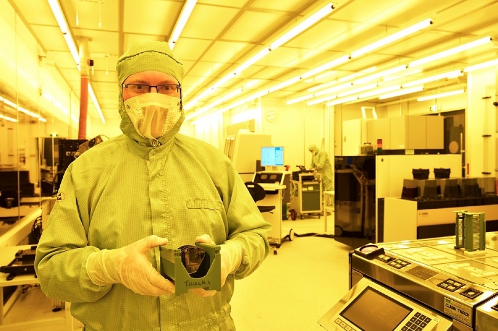
By 2030, PhotonDelta intends to have created a pan-European integrated photonics industry that will churn out 100,000 wafers a year, reports Rebecca Pool. [Image: Luc Augustin, CTO of Smart Photonics, with a wafer containing photonic chips. (Bart van Overbeeke)]
In April this year, PhotonDelta, of The Netherlands, secured a mighty €1.1 billion in public and private funds to kick-start a pan-European integrated photonics industry. By 2030, the photonics umbrella organisation, which provides InP, SiN and silicon photonics production and prototyping facilities, aims to have created an 'ecosystem' of hundreds of companies delivering more than 100,000 wafers per year, and photonics-related products, to industries worldwide.
As PhotonDelta chief executive, Ewit Roos, highlights, funds will be invested in photonics start-ups and other businesses to scale activities, expand production and research facilities, attract engineers and also to develop, what he describes as, a 'world-class' design library.
“Two to three years ago no-one spoke about strategic autonomy in Europe but the current chip shortage and today's geopolitical situation have triggered European policymakers to make sure we are not dependent on Asia and the US for this key technology,” highlights Roos. “As well as this, we've also seen a need to accelerate the development of photonics technologies in The Netherlands and the rest of Europe.”

PhotonDelta chief executive, Ewit Roos.
Indeed, thanks to the likes of Philips and Mathworks, The Netherlands has a rich heritage in tech research and development, with myriad home-grown start-ups already forming the basis of a photonics supply-chain. For example, in The Netherlands alone, LioniX International, Bright Photonics and Smart Photonics have been pushing back the boundaries of photonics design and fabrication while Phix has been developing photonic integrated circuit (PIC) packaging processes.
Staying in The Netherlands, start-ups and scale-ups such as Surfix, MantiSpectra, Quix, Effect Photonics, and so many more, have developed PICs for a broad range of applications whilst across Europe, a vast array of start-ups including aiXscale Photonics, Germany, and Ommatidia LiDAR, Spain, have been following similar trajectories. What's more, Belgium-based imec is also home to SiN and SiPh platforms for CMOS-compatible PIC fabrication, and joint European platform for photonic integrated components and circuits, JePPIX, can be used to develop prototypes based on InP and SiN photonics.
“In The Netherlands, we are strong in research, photonics integration and parts of [photonic chip] manufacturing but you need all kinds of other expertise to make photonic integrated circuits,” says Roos. “At PhotonDelta, we want to bring all of this together and increase the pace of development for photonics manufacturing, in both the front-end and back-end... My dream is that we do for photonic integrated circuits what TSMC has done for today's electronic ICs.”
Planning the future
Since 2019, PhotonDelta has been investing in in many start-ups, including Effect Photonics, to develop its DWDM optical SoC technology, Phix, with its high volume PIC back-end foundry packaging facility, and Smart Photonics and its InP foundry processes. Looking forward, investment will continue up and down the integrated photonics supply chain, but at faster pace. Roos points to InP production at Smart Photonics' foundry, SiN PIC development at LioniX, and quantum photonic processor development at QuiX, also of The Netherlands, as just a few investment targets.
Along the way, PhotoDelta has also been offering the legacy semiconductor industry practice of Multi Project Wafer runs with partners, Smart Photonics, LioniX, imec and JePPIX, to reduce the cost of PIC prototyping. “All these players will be receiving a lot of support from us, and it's also important that we work with imec, as we will then have all the important platforms; CMOS, silicon photonics, InP and SiN,” points out Roos. “We're not necessarily doing anything new with these firms, but we are accelerating activities.”
Critically, Roos is keen to ensure that large-scale photonics production is reliable, stable and robust. Looking at wafer production, some 5000 four-inch InP wafers are currently being manufactured at Smart Photonics, but Roos anticipates some 100,000, six-inch InP wafers being produced every year come 2030. LioniX could also be churning out up to 50,000 eight-inch SiN wafers, a year, by the same time.

A quantum photonic processor from QuiX, of The Netherlands. [Daniel Verkijk, QuiX Quantum]
Meanwhile, Roos hopes to achieve fully-automated, higher speed back-end production come 2030 with a comprehensive design library and using automated wafer-scale, generic, integration technology across silicon, silica and InP substrates. “You can only survive if you have a world-class library of building blocks that can be used in manufacturing,” he says.
“We have put a lot of emphasis, in the next six years, on application technology,” he adds. “And to be more focused on what high volume customers require for next-generation applications, be it for automotives, biosensing, agriculture, quantum photonics – you name it.”
Clearly, a solid pan-European photonics integration supply chain will demand an equally solid workforce. Roos is confident this will follow, and highlights how Dutch photolithography systems manufacturer, ASML, attracts tens of thousands of job applications every year thanks to its attractive working environment and conditions. Still, the PhotonDelta chief executive is keen to keep an eye on the rest of the world.
“European sovereignty doesn't mean you have to have all of your volume production capacities within European borders – that would be insane and against all economic rules,” he says. “But we need to have strategic assets within our borders so the world also comes to us – and for us, this will be photonics integrated circuits and photonics engines.”


