Optimising GaN crystal growth
Very high temperature oxygen vapour phase epitaxy looks to simplify bulk GaN crystal growth
Engineers from Japan have improved the quality of GaN crystals produced with oxygen vapour phase epitaxy by shifting growth to very high temperatures.
Their success increases the promise of the oxygen vapour phase epitaxy technique (OVPE), which delivers several advantages over the incumbent, HPVE.
Benefits of OVPE over HVPE include the absence of solid by-products, such as NH4Cl, and the production of material with a high carrier concentration and low resistivity, thanks to the incorporation of a high concentration of oxygen, which acts as a donor.
Spokesman for the Japanese team, Shigeyoshi Usami from Osaka University, told Compound Semiconductor that the key to the latest breakthrough has been the establishing of a pre-growth technology.
“Since GaN decomposes at 1300 degrees Celsius, it was very difficult to grow at such a high temperature,” explains Usami.
However, Usami says that by introducing a pre-growth process, he and his co-workers can now suppress the decomposition of the seed substrate and grow GaN at 1300 degC.
When these engineers were previously restricted to a growth temperature of 1250 degC, they produced polycrystalline GaN at a growth rate of around 100 µm/hr. When cranking up the temperature to 1300 degC, they almost eliminated polycrystallinity, while doubling the growth rate.
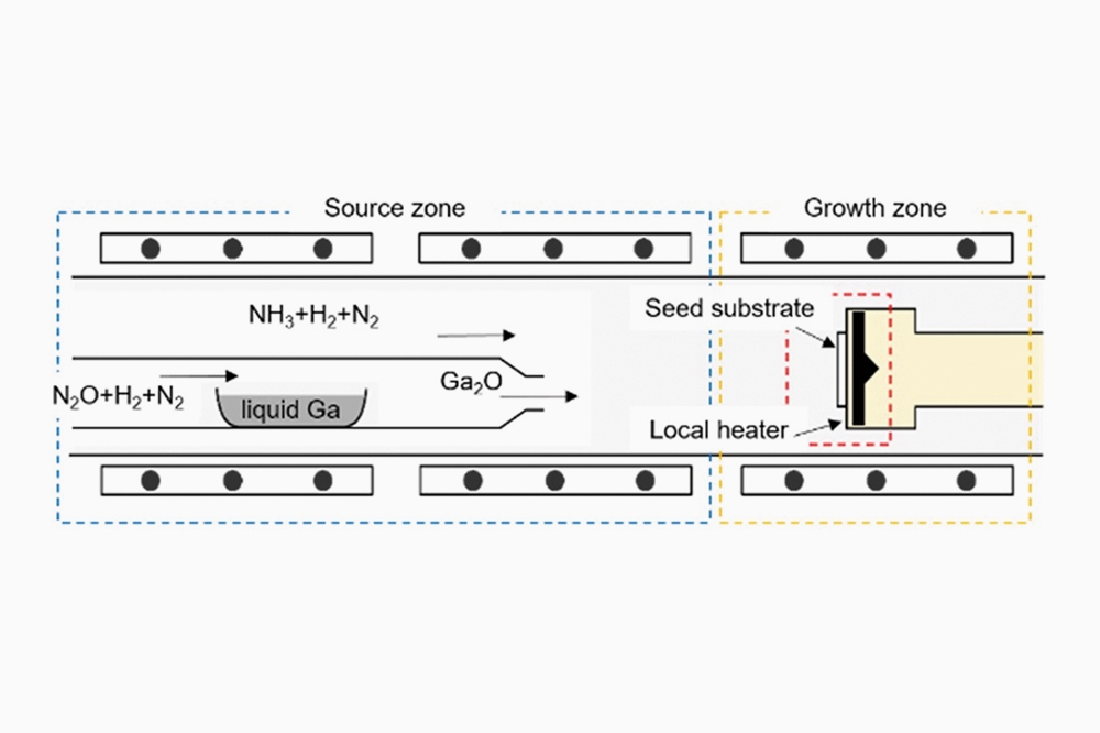
With OVPE, GaN is produced by reacting gallium oxide and ammonia; water and hydrogen are the by-products. Gaseous gallium oxide is formed by oxidising gallium pellets.
To produce bulk GaN, the gallium oxide and ammonia are directed at a GaN seed that is placed in the growth zone and heated with a resistive heating system (see Figure).
Once the temperature of the seed exceeds 500 degC, ammonia is directed at its surface to prevent GaN decomposition. However, this is not sufficient when the temperature of the seed is as high as 1300 degC. At that temperature voids form at the interface between the seed and epi-layer.
In this latest work, Usami and colleagues show that introducing Ga2O3 gas during the heating-up period prevents decomposition of the seed at 1300 degC. Initial success came from using a Ga2O3 flow rate of 2.1 sccm for heating between 1200 degC and 1250 degC, before increasing to 4.2 sccm over the 1250 degC to 1300 degC range.
Scanning electron microscopy images show that GaN grown with these conditions is free from large pits, polycrystallinity and voids at the interface between the seed crystal and the epilayer. These findings indicate that Ga2O3 gas flow prevents decomposition of the seed prior to GaN epigrowth.
A second set of experiments considered the impact of temperature on the extent of polycrystallinity at high grow rates. The researchers compared growth at 1200 degC, without any pre-growth flow of Ga2O3 gas; growth at 1250 degC, using a Ga2O3 flow rate of 2.1 sccm when heating between 1200 degC and 1250 degC; and the conditions previously used for growth at 1300 degC.
Scanning electron microscopy images of a number of samples produced during this study showed that at 1200 degC and 1250 degC, the higher the Ga2O3 gas flow during GaN growth, the greater the extent of polycrystallinity. However, at 1300 degC the polycrystalline density did not increase with Ga2O3 gas flow, and GaN with almost no polycrystallinity could be produced at a growth rate of 195 µm/hr.
Usami thinks that it will be possible to grow GaN at even higher temperatures, such as 1350 degC, which will help to accelerate growth.
“But, the higher the temperature, the more severe the decomposition, so it is necessary to precisely optimize the pre-growth conditions.”
The team is aiming to realises growth rates of over 1 mm/hr.
Reference
A. Shimiz et al. Appl. Phys. Express 15 035503
Picture Caption: With oxygen vapour phase epitaxy, GaN is produced by reacting gallium oxide and ammonia. Water and hydrogen are by-products.


