Ayar Labs and Nvidia collaborate

Ayar Labs’ optical I/O unleashes the potential of next-generation AI compute architectures
Ayar Labs, a chip-to-chip optical connectivity company, is working with Nvidia to develop infrastructure based on optical I/O technology to meet future demands of AI and high performance computing (HPC) workloads.
The collaboration will focus on integrating Ayar Labs’ technology to develop scale-out architectures enabled by high-bandwidth, low-latency and ultra-low-power optical-based interconnects for future Nvidia products. Together, the companies plan to accelerate the development and adoption of optical I/O technology to support the explosive growth of AI and machine learning (ML) applications and data volumes.
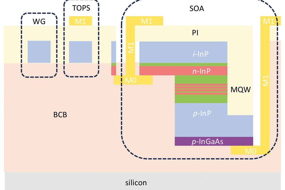
Ayar Labs’ patented approach uses industry standard silicon processing techniques to develop high speed, high density, low power optical-based interconnect 'chiplets' and lasers to replace traditional electrical based I/O.
Optical I/O changes the performance and power trajectories of system designs by enabling compute, memory and networking ASICs to communicate with increased bandwidth, at lower latency, over longer distances and at a fraction of the power of existing electrical I/O solutions. The technology is also foundational to enabling emerging heterogeneous compute systems, disaggregated/pooled designs, and unified memory architectures that are critical to accelerating future data centre innovation.
“Today’s state-of-the-art AI/ML training architectures are limited by current copper-based compute-to-compute interconnects to build scale-out systems for tomorrow’s requirements,” said Charles Wuischpard, CEO of Ayar Labs. “Our work with Nvidia to develop next-generation solutions based on optical I/O provides the foundation for the next leap in AI capabilities to address the world’s most sophisticated problems.”
“Over the past decade, Nvidia-accelerated computing has delivered a million-X speedup in AI,” said Rob Ober, chief platform architect for Data centre Products at Nvidia. “The next million-X will require new, advanced technologies like optical I/O to support the bandwidth, power and scale requirements of future AI and ML workloads and system architectures.”
As AI model sizes continue to grow, by 2023 Nvidia believes that models will have 100 trillion or more connections – a 600 times increase from 2021 – exceeding the technical capabilities of existing platforms. Traditional electrical-based interconnects will reach their bandwidth limits, driving lower application performance, higher latency and increased power consumption. New interconnect solutions and system architectures are needed to address the scale, performance and power demands of the next generation of AI. Ayar Labs’ collaboration with Nvidia is focused on addressing these future challenges by developing next-generation architectures with optical I/O.


