
A step closer to next-generation semiconductors?
Korean team selectively controls electrical properties of semiconductor devices using Cl-doped tin diselenide
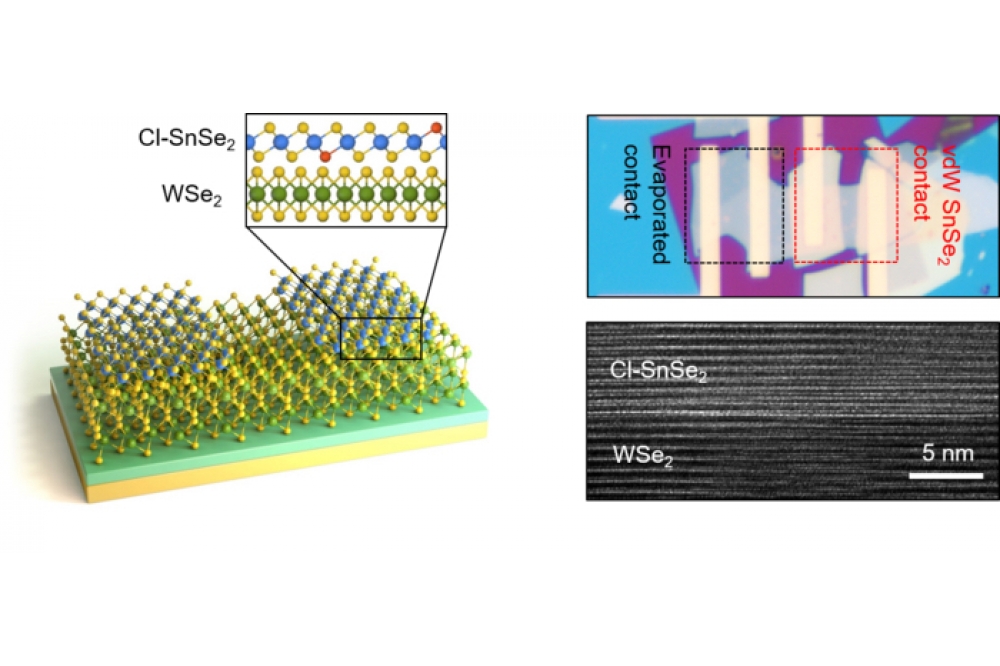
The Korea Institute of Science and Technology (KIST) has announced that a joint research team led by Do Kyung Hwang of the Centre for Opto-Electronic Materials and Devices and Kimoon Lee of the Department of Physics at Kunsan National University, has succeeded in implementing 2D semiconductor-based electronic and logic devices, whose electrical properties can be freely controlled by developing a new ultra-thin electrode material (Cl-SnSe2).
The joint research team was able to selectively control the electrical properties of semiconductor electronic devices using Cl-doped tin diselenide (Cl-SnSe2), a 2D electrode material.
The researchers say it is difficult to implement complementary logic circuits with conventional 2D semiconductor devices because they only exhibit the characteristics of either n-type or p-type devices due to the Fermi-level pinning phenomenon.
In contrast, if the electrode material developed by the joint research team is used, it is possible to freely control the characteristics of the n-type and p-type devices by minimising defects with the semiconductor interface. In other words, a single device performs the functions of both n-type and p-type devices. Hence, there is no need to manufacture the n-type and p-type devices separately.
By using this device, the joint research team successfully implemented a high-performance, low-power, complementary logic circuit that can perform different logic operations such as NOR and NAND.
Hwang said that, “this development will contribute to accelerating the commercialisation of next-generation system technologies such as artificial intelligence systems, which have been difficult to use in practical applications due to technical limitations caused by the miniaturisation and high integration of conventional silicon semiconductor devices."
He also anticipated that "the developed 2D electrode material is very thin; hence, they exhibit high light transmittance and flexibility. Therefore, they can be used for next-generation flexible and transparent semiconductor devices."
Reference
'Fermi-Level Pinning-Free WSe2 Transistors via 2D Van der Waals Metal Contacts and Their Circuits' by Jisu Jang et al; Advanced Materials (2022)


