The secret sauce of silicon carbide wafer success
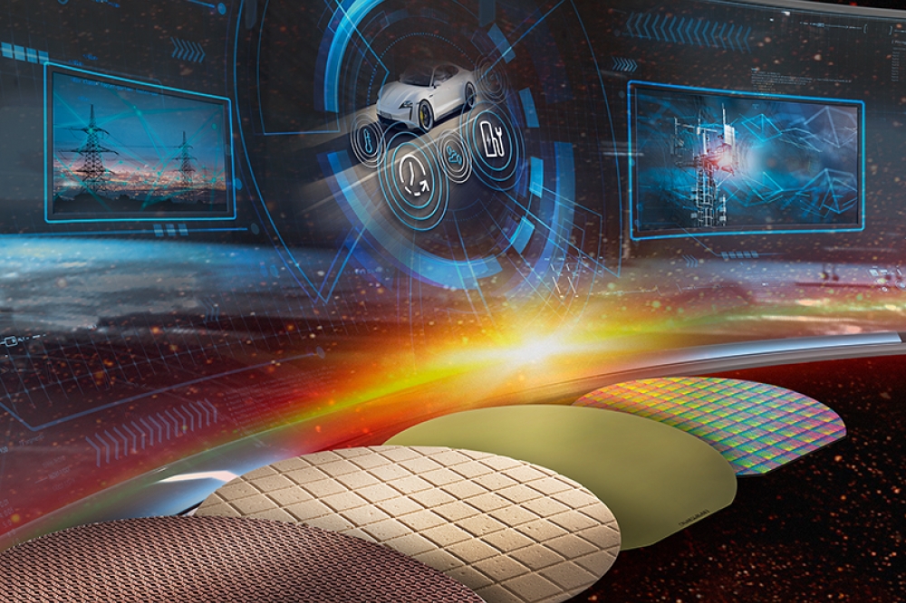
Nearly all devices we use today depend on semiconductors. New technical
advancements and requirements necessitate the use of silicon carbide
(SiC) for many demanding semiconductor applications. Due to its physical
and electronic properties, SiC based devices are well suited for high
temperature and high-power/high-frequency electronic devices enabling
the advancements in Electric Vehicles (EVs), 5G and IOT technologies.
While they bring a lot of benefits for the end-user, the production of
high-quality SiC substrates presents many challenges to wafer
manufacturers. Pureon has been providing state-of-the-art solutions to
SiC wafer manufacturers for over 15 years in the various process steps
of slicing and surface finishing.
BY DR. WILLIAM GEMMILL, TERRY M. KNIGHT, DIPL.-ING. HELGE WILLERS, DR. RAVI BOLLINA AND ARTHUR LENART FROM PUREON
Living has become smarter! Our day starts with the alarm from our smartwatch. We clap our hands to turn on the light in our smart home. While we wait for the coffee machine to make our coffee, we check our smartphone for the latest news and updates. Then we unplug our electric vehicle from the charger and drive to work. At work we do our job by being connected to the whole world with the help of cloud-based computers and audiovisual communication systems.
Semiconductors improve our daily lives
We have followed Gordon Moore’s Law to once unimaginable levels, and semiconductors have revolutionized the way we work, communicate, travel, entertain, harness energy, and treat illness. They not only make useful devices of our daily life possible, but also make them more compact, less expensive, and more powerful. Take for example the evolution of mobile phones: The first devices in the 80s were very heavy, cost nearly as much as a car, and held a charge for only about 30 minutes of talk time. Today, our smartphones are highly intelligent mobile devices, nearly as powerful as a regular computer and are available for everybody. Amazingly, the greatest potential still lies ahead. As the building blocks of technology, SiC based semiconductors will continue to enable great breakthroughs: from aerospace and consumer electronics to energy and medicine – entire industries will be transformed. A good example for this transformation is the automotive industry. Electric vehicles have evolved from an ecological niche product to a preferred everyday alternative. This development was supported by more powerful electric drivetrains, using higher currents and more effective circuits. This is where Silicon Carbide plays a dominant role.
Why Silicon Carbide?
The answer is quite simple: more power, higher efficiency and better reliability at higher voltages. There is a transformation not only in the industry but also of semiconductor materials itself. To handle the increased requirements of electric devices, SiC has become the preferred substrate material for advanced semiconductors, especially for power electronics. It allows a 10x higher dielectric breakdown field strength, 15x higher breakdown voltages and offer 3x higher thermal conductivity. In addition, SiC enables higher operating temperatures (up to 400°C vs 150°C for Silicon) and has a 2–3 times higher current density.
The ability of SiC semiconductors to perform at high temperatures, voltages and power has resulted in its increased demand in multiple industries. Data centers for example use SiC for power supplies enabling substantial reduction in power required for cooling systems.
In addition, uninterruptable power supply (UPS) systems ensure a stable, consistent source of power. Another example are 5G base stations: they process an increasing amount of data resulting in a rise of power requirements. SiC semiconductors are used for MHz switching and deliver increased power at a reduced size.
Breakthrough for electric vehicles thanks to SiC
Especially the automotive industry benefits from the advantages of SiC. Thanks to the higher efficiency of SiC semiconductors, manufacturers like Porsche were able to make the transition from 400 V to 800 V batteries. This results in faster charging times, smaller batteries and longer ranges. Other applications that benefit from SiC:
⊕On-board battery charger: Converts the external AC into DC to charge the battery and can double the power in half the size
⊕On-Board DC/DC Converter: Converts the on-board battery voltage into a clean ~12VDC bus to power on-board equipment
⊕Powertrain: The inverter, electric motor, and its mechanical attachment to the driveline. Switching losses to less than 80% with 30% smaller size. Results in a smaller battery (less weight, less heat) and longer range
⊕Off-Board DC fast charger: Faster DC charge stations for rapid recharging
Challenges for the industry
As the demand over the next five years is expected to increase massively, the main challenge for the industry is not only the sheer volume of wafers required but also the changing specifications of the wafers to reflect those of silicon wafers. Tighter tolerances and specifications will push current and future manufacturing methods. Innovation will be critical to overcome these challenges. Taking a proactive approach to anticipate shifts in manufacturing technologies requires developing a deep relationship with process engineers and R&D based upon trust and know-how to develop next generation products.
SiC substrate manufacturers have the drive to improve process efficiency and reduce wafer production costs because the market is striving for power device price parity with Si based devices. Furthermore, the enormous growth in demand (production ramps, new facilities, etc.) and the navigation of global supply chain constraints amidst a surge in demand for both SiC based applications and an overall surge in demand for all types of semiconductors requires innovation in the manufacturing processes.
Optimizing costs from the beginning
Cost per wafer will become a driving factor when developing or optimization of a process step. Most will look to decrease process times, or cheaper consumables, thinking that will drive down the cost. As SiC is increasingly adopted in device manufacturing and moving from a R&D material to commercialization, increase in yield is where a significant improvement in cost of ownership will be achieved. Maximizing yield while minimizing rework, will increase throughput on existing processes.
A major challenge for the industry is the lack of availability of reliable partners for providing surface finishing solutions in manufacturing processes. Unproven solutions and unreliability in new vendors cause the risk of slowing or even halting production or scale-up efforts. This often leads to long lead times for consumables, tools and customer qualification which is a massive hindrance to expand production capacity. That is why consumables have an impact on the whole process. The consistency of pads, slurries and templates run-to-run and lot-to-lot is critical in this effort in optimizing yields.
PUREON- A total process solution provider for silicon carbide wafering
Pureon has many years of experience in the semiconductor industry and has developed proven solutions for wafer production. Pureon supports manufacturers to establish reliable and efficient processes. Pureon’s semiconductor history with two decades of developing products for the SiC market, contributes to overcoming the critical manufacturing challenges.
Early engagements with customers in their roadmaps to identify bottlenecks, define resources and expectations is critical. As a consumable manufacturer with in-house wafer processing capability, Pureon is able to conduct testing and generate data with its own polishing and surface laboratories. This capability provides both Pureon with significantly shorter development cycle times and customers with representative data to mitigate risk in the testing and qualification of new products. This benefits wafer manufacturers by shortening the testing and acceptance at their sites. Pureon teams up with OEM's to run full scale tests to confirm findings. This removes the challenge of a customer having to take a tool or cell out of production to do testing and collect data to compare to current process of record.
Optimizing current and developing new processes
A major challenge for the industry is the limited availability of ingots and wafers, thus increasing the demand to ship anything that can be made. This has emphasized the importance of efficient and reliable production processes. However, any process change could lead to a full requalification, which could take months. Therefore, manufacturers have the drive to optimize their current production processes to benefit from lower process costs. Pureon supports this effort in supplying solutions that extend consumable lifetimes and shortening cycle times, while optimizing and improving yields.
At the same time the market requirements are changing. Hence, the industry is migrating closer to prime silicon wafer specs, requiring manufacturers to develop new processes. A good example is the move from 150 mm to 200 mm wafers, requiring completely different manufacturing flow and equipment. To realize high volume manufacturing processes for these new requirements, new manufacturing technologies are being introduced in all process steps. Pureon’s focus on innovation and forward-looking development strategies are uniquely positioned to provide SiC wafer manufacturers with next-generation solutions, supporting the market’s maturation through increasing productivity and reducing cost of ownership.
Multi-wire saw processing of SiC ingots – secret sauce for optimum ingot slicing
To prepare SiC substrates for device fabrication one must first cut wafer blanks from the single crystal or ingot. The primary way to do this is through the use of a multi-wire saw that utilizes a thin wire moving at high speeds in combination with a diamond abrasive slurry to precisely cut wafer blanks from the SiC ingot. Major inputs to this process include speeds and feeds, type and size of wire, and the properties of the diamond abrasive slurry. The quality of the cut is judged in the responses of wafer shape, namely bow, warp and total thickness variation (TTV). Successfully cutting high quality blanks at the wire saw step is arguably the most important step of the wafer production process, as downstream improvements in wafer shape are very difficult to achieve.
Pureon provides solutions for the wire saw process in the form of the diamond abrasive slurry and close collaboration with wire saw OEMs as well as customers to optimize this process. Within the wire saw slurry consumable space there are two types: oil-based and non-oil-based formulations. Pureon offers both oil-based (WSO) and non-oil-based (WSG) slurry solutions. Pureon proprietary chemistry and classified diamonds in the slurries provide lot-to-lot consistency which translates to reproducible processes at the customers’ site. Furthermore, this eliminates the need to in-house mix wire saw slurry and reduces overhead. Whether it is the first wafer or the 1000th wafer, the properties of the TTV, bow, warp and surface quality are precisely controlled. Hence improving the yield and quality of the wafers.
Exciting opportunities for multi-wire-saw processes
Pureon’s latest advancements in wire saw slurry offerings are exhibiting exciting opportunities to improve bow, warp, and TTV compared to existing solutions, all while reducing the environmental and occupational hazards associated with traditional oil-based slurries. Recent advances in non-oil based slurry formulation designs are proving to provide excellent wafer quality. These solutions are enabling customers to produce higher quality wafers off the saw, setting their subsequent processing up for success as seen in Table 1.
Diamond mechanical polishing of SiC wafers
The next major process in the manufacture of SiC substrates is the mechanical polishing of the wafers using a polishing slurry containing diamonds and a polishing pad. Typical processes are performed on either double side, single side or some combination of double and single side polishing tools. The output from this process step is to present a very flat and relatively low roughness wafer to the final polishing operation.
Critical inputs include the proper selection of diamond based polishing slurry and polishing pad, processing parameters such as polishing pressures, and table speeds, as well as machine selection. Of the critical inputs, the polishing slurry and pad contribute the most to a successful process optimization. Pureon has identified optimum process solutions when it comes to providing customers with maximum process performance in terms of material removal rates, wafer shape, and surface quality, by marrying the appropriate polishing pad and polishing slurry with respect to installed tooling. Pureon’s extensive experience in the processing of SiC wafers via diamond mechanical polishing can be leveraged to maximize process efficiency no matter the tool set in customers facilities. Table 2 describes the DMP process flow for bulk and fine removal steps.
Diamond based slurry development has, over the years, been a major focal point for Pureon’s innovation team. The company has identified highly optimized formulations that allow for modulation of material removal rates on the different faces of the SiC substrates. Pureon identified diamond types that work synergistically with the appropriate polishing pads and process parameters that continue to extract more performance from this process and drive efficiency gains, see for example Figure 1. Pureon sees great opportunity in driving down cost of ownership for this process step as the 150mm SiC substrate market matures in the coming years.
Chemical mechanical polishing of SiC wafers
The final major process of SiC wafer production is typically referred to as the chemical mechanical polishing (CMP) step. This process step aims only to prepare the substrate surface for epitaxial growth, while imparting zero or as little as possible change to wafer shape. This is typically achieved using a highly reactive chemical based polishing slurry and a polyurethane based or a urethane impregnated felt type of polishing pad to remove only a few microns from the wafer surface. Wafers are delivered to the polishing pad and held in place via a template or wafer fixture in single-side batch tools or via vacuum chuck with a backing film in single-wafer tools. The materials used in these wafer carriers are exposed to the highly reactive chemistry of the polishing slurry, thus requiring robust tolerance to the reactive chemistry.
WSG is an advanced glycol based diamond suspension for multi wire saw slicing of SiC boules- with proprietary additives for enahnced stability of the suspension.
Pureon continues to develop advanced wafer carriers and films for use in this process to extend the service life, resulting in improved cost of ownership. Pureon has also worked closely with the industry to bring two new polishing pads for SiC CMP to the market as recently presented at the 2021 ECSCRM in Tours, France. These next generation CMP polishing pads are enabling higher productivity and increased quality from the CMP process. The formulation of final polishing slurries has been the subject of extensive research over the years, and innovation continues in this area. Therefore, it is critical for optimization to have a deep understanding of the interactions between the different consumables combinations in this process step. Pureon works closely with final CMP slurry providers to couple their technology with the optimum polishing pad, pad conditioning process and wafer templates or carrier films. Advancements in final CMP polishing pad technology continue to drive increases in productivity. Pureon continues to drive innovative solutions for consumables and processes for the final polish of SiC wafers.
Figure 1. Representative silicon face MRR (mm/h) response surface in a three component mixture design using 3 mm monocrystalline diamond.
Driving into the future with Pureon
The growth of the SiC device market requires significant advancements in substrate manufacturing, both in the current state and in the development of next generation substrates. Pureon has been supporting the SiC wafering industry for almost 20 years with their knowledge, solutions, and experience in this market. Their experts continue to innovate, to improve substrate yields and lower the cost of SiC wafers, thus enabling a faster adoption of this technology. Pureon drives SiC manufacturing to new limits, enhancing all our lives. That's why innovation and pushing the limits never ends at Pureon. Learn more about their newest solution for lapping SiC wafers using the new pad IRINO-PRO-C. More details and technical presentations will be made during the ICSCRM in Davos, Switzerland, from 11 - 16 September 2022


