Venturing to Venus

SiC unlocks the door to uncooled electronics that’s capable of handling the extreme temperatures found on Venus
BY Carl-Mikael Zetterling and Mattias Ekström from KTH Royal Institute of Technology
Is there life beyond Earth? And if so, how intelligent is its form? These are two intriguing questions, piquing the interest of much of humanity. In a search for answers, we have built ever more powerful telescopes that probe into the deeper reaches of the universe, and embarked on missions to nearby planets, to examine what they are made of.
Why Venus?
In the last few years there has been much interest in Venus. Back in 2020, scientists uncovered possible signs of life in its cloud layers, evidenced by traces of phosphine that could not be explained in other ways. This has spurred the planning of a number of missions to this second planet from the Sun. NASA has two tentative trips scheduled for 2028-2030: one is entitled DAVINCI+, short for Deep Atmosphere Venus Investigation of Noble gases, Chemistry, and Imaging; and the other is VERITAS, and acronym for Venus Emissivity, Radio Science, InSAR, Topography, and Spectroscopy. The European Space Agency also has Venus on its agenda, through a project called EnVision, which will investigate the atmosphere, surface and sub-surface of this planet; and there is a private mission planned by Rocket Lab, slated for 2023 – a probe will analyse Venus from an altitude of 30 miles, scrutinising atmospheric layers for phosphine and hunting for proof of previous life.
Missions to Venus are certainly not new. There were many between 1960 and 1981, involving fly-by, orbiters, probes and landers. These efforts established that the surface temperature of this planet is as high as 460 °C, which makes exploration extremely challenging. Between 1976 and 1981 the Soviet Union put a number of Venera landers on the surface, equipped with heat shielding for the silicon electronics. But even with this assistance, the electronics only survived for up to two hours (although that mission still provided colour images of the surface).
The benefits of developing electronics that is capable of handling the extreme temperatures found on Venus would actually accomplish far more than simply determining whether Venus ever supported life. Success on this front would also help us to understand far more about the nature of our own planet. Why? Well, Venus is similar in size to Earth, and it has an atmosphere containing 96 percent CO2. Consequently, understanding the climate of Venus could help us to understand what is happening at home, by providing a second reference point that would improve our computer models. Armed with more rigorous, reliable models, we would be in a better position to understand our atmosphere’s composition and temperature variations.
Efforts at gaining a better insight into Venus’ climate must consider whether this planet still has active volcanoes. This is an outstanding question with important implications, as active volcanoes offer one explanation for the planet’s sulphuric acid content. One way to detect volcanic activity is to use seismometers, which would require another lander mission to Venus. However, if this is to be of value, the electronics in the seismometer would need to survive 2 months or 2 years, rather than just a couple of hours.
A block diagram of the proposed Venus Lander. This should be seen as an
example of the electronic building blocks needed for a typical system.
Different sensors are used, and amplifiers are needed in many cases to
increase the signal level, prior to conversion to a digital signal in an
Analogue-to-Digital Converter (ADC). The microcontroller (MCU) with
memory stores the data until it can be sent to a satellite for relaying
to Earth. The radio transceiver activates when the satellite is in
range, with the microcontroller sending stored data. The power supply
unit (PSU) converts energy for different parts, and turns off units when
not used. One possible high-temperature power supply would be a
Radioisotope Thermal Generator (RTG).
Why is there a temperature limit?
All classes of semiconductor have an intrinsic temperature limit. Heating this material generates carriers, in the form of electron-hole pairs. For devices at room temperature, these carriers are hardly noticeable, except in sensitive systems where there is added noise – it is for this reason that radio telescope receivers are cooled. At elevated temperatures leakage currents escalate, causing some sensors to lose their sensitivity, power consumption to increase, and most transistors to operate less optimally. At even higher temperatures far greater issues arise, with semiconductor devices no longer able to block the applied voltage and catastrophic failure occurring. To try and prevent this from happening, in many high-power electric circuits heat sinks and fans extract the heat from the devices.
Why SiC?
Governing the operating temperature of every semiconductor device is its bandgap. The thermally generated carriers – referred to as the intrinsic concentration in physics text books – depend on the energy bandgap in an exponential relation, causing the increase of conductivity to rise exponentially with temperature.
Due to this relationship between the bandgap, the temperature and the conductivity, SiC is far better than silicon at handling the heat. SiC is blessed with a bandgap of 3.2 eV, compared with just 1.12 eV for silicon. Thanks to a tripling of the bandgap, devices made from SiC can operate at up to at least 800 °C, compared with around just 200 °C for silicon. What’s more, the wider bandgap reduces sensitivity to radiation damage.
Right now, sales of SiC devices are ramping fast, with SiC MOSFET switches and power Schottky diodes winning substantial sales, thanks to their capability to operate at high voltages with low on-state and switching losses. Compared with incumbent silicon devices, those made from SiC benefit from a critical field for breakdown that is almost ten times higher, allowing the device’s blocking region to be ten times thinner and have almost a hundred times higher doping. The upshot of these attributes is that, for the same blocking voltage, SiC devices have an on-resistance that is 200 to 400 times lower than their silicon siblings. Many manufacturers are offering SiC diodes and transistors rated between 600 V and 3300 V, which are being deployed in power supplies and electric vehicles.
A sample SiC chip with all the developed circuitry. The rather massive
leads encircling the individual circuits are power conductors. While BJT
circuits take more current than those based on MOSFETs, chip heating is
not a problem on Venus. Photo: Jörgen Städje.
Our solution
Our team at KTH Royal Institute of Technology, Sweden, has spent several years developing SiC electronics that is capable of handling the high temperatures found on the surface of Venus. We have taken a slightly different approach from what you might expect, shying away from using MOSFETs, the most common form of transistor deployed in today’s ICs. That’s because MOSFETs are impeded by a relatively high level of vulnerability to the gate oxide, and a threshold voltage that varies by -1 V for an increase of 100 °C. A better option is the bipolar junction transistor (BJT), which offers a performance that changes far less with temperature – for instance, the built-in voltage of the p-n junctions shifts by just -0.2 V for an increase of 100 °C. Using the BJT, we are able to design all the circuits we need, drawing on advice provided in text books from the 1960s.
ICs also require resistors and capacitors, which can be made using the process steps employed for making the transistors. We avoid ion implantation, because this introduces electron-hole recombination centres. Instead, we define all our doped regions with the combination of epitaxial growth of SiC layers and dry etching, which defines the geometry of the features.
During our campaign, we have developed a self-aligned method to form contacts. We use SiO2 to isolate the components and the two metal layers from one another. To produce a flat surface, we have turned to chemical mechanical polishing, due to the large variation in topography after dry etching.
A minimum embedded system for a Venus lander typically has: sensors to measure temperature, seismic activity and UV light; amplifiers to increase the signal level; analogue-to-digital converters, to convert to digital values that can be stored; a microcontroller (MCU) with memory (SRAM) to collect data and communicate; a radio transceiver to communicate with an orbiting satellite; and a power supply unit.
During our five-year project Working on Venus, which started in 2015, we have built and demonstrated circuits separately, with PhD students taking responsibility for separate parts. Crucial overarching requirements during this effort were that: the process design would include all components; the process design kit would be used to handle the simulation models of the transistors for temperatures up to 500 °C; and the construction of the larger circuits would draw on standard design-rule-checking and layout, while comparing with schematic checkers.
Cross-section and top view of the integrated circuit elements used: the
transistor, the resistor and the capacitor. These components are
isolated from each other using a p-n junction beneath the collector
region, and SiO2 in the trenches etched between the components. Around a
dozen mask layers are required for the full process with two metal
interconnect layers.
Did we succeed?
Our efforts have paid substantial dividends, enabling us to demonstrate separately all the parts in the block diagram up to 500 °C. This success has provided a foundation for making several amplifiers, since different sensors need different impedance matching. We have also made Flash and successive-approximation ADCs. Our efforts have not had to include developing either gas- or temperature sensors, as both were available prior to our project. We have confirmed that suitable seismic sensors can be made using silicon, if the readout electronics is made in SiC. In addition, we have demonstrated radio circuits. This is not easy, with characterisation of a 59 MHz signal at 500 °C challenging, as normal coaxial cables and connectors cannot be used. We have also investigated the capability of non-volatile ferroelectric memory, in the form of thin-film vanadium-doped bismuth titanate.
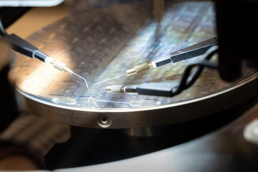
The most challenging construction was the microcontroller with SRAM, due to the large number of transistors involved. As a standard package can’t withstand high temperatures, we wanted to measure our circuits on-wafer. Unfortunately, this limits the number of needle-probes we can use in our setup to around a dozen, an issue we address by introducing a 4-bit external bus. The other connections were for the power supply and ground, the two-phase clock, and other control signals.
One task we still need to tackle is to improve the temperature stability of the metallisation system. Currently we employ aluminium, which melts at 660 °C. If we could switch to an interconnect system using a refractory metal, such as tungsten, this would enable electronic circuits to operate at even higher temperatures. According to demonstrations at NASA, SiC circuits can operate at 800 °C, even for extended time.
A circuit featuring a 4-bit microcontroller with SRAM. It consists of
5900 transistors and 3900 resistors, and draws 1 A at 15 V. There are
many silicon microcontrollers that are more efficient, but this one
works at 500 °C. A 4-bit external bus allows on-wafer probing on the hot
stage. Photo: Shuoben Hou.
While we have shown that an entire uncooled electronic system operating at very high temperatures can be built using SiC, packaging these devices is an entirely different story. Plastic packages are not an option, as they will not work above 125 °C. Far more promising are ceramic packages, but they are not generally characterized for temperatures above 230 °C. This, though, is a chicken-and-egg problem: there is no drive to design and characterise such packages until there is commercial need for them, while it’s not possible to commercialise high-temperature electronics until there are high-temperature packages. For our high-temperature characterization of radio circuits, we use custom-made low temperature co-fired ceramic carriers to mount the SiC transistors.
Hot stage with needle probes to measure electrical characteristics from
room temperature to 600 °C on SiC wafers. Photo: Jörgen Städje.
Fortunately, packaging need not be an insurmountable problem. What’s more, even though Venus’ atmosphere cannot be kept out of the lander structure, as it’s composed of mainly CO2 it will not attack the circuitry. Note that the surface pressure is of no importance.
We would be delighted to participate in one of the missions to Venus. But that’s not our only goal – there are also opportunities for us associated with terrestrial applications. To that end we have also made a 555 timer from SiC. It operates at up to 500 °C, and can be used for timer, delay, pulse generation and oscillator applications. In addition, we have been collaborating with researchers at University of Arkansas in Fayetteville, who have been using our models and process technology to design high-temperature ICs for geothermal and space applications.
Scanning electron microscopy image of a non-volatile ferroelectric
capacitor using thin-film BiTV (vanadium-doped bismuth titanate). The
inset shows the optical photograph.
- Shuoben Hou is acknowledged for manufacturing the SiC wafers, and Muhammad Shakir is acknowledged for making the process design kit and drawing the lithography masks. Jörgen Städje is acknowledged for the photographs and encouraging our work.
Further reading
The full PhD theses of several of the PhD students (Ekström, Hou, Shakir, and Waqar) in the Working on Venus project is available from www.workingonvenus.se; previous work from KTH on high temperature SiC circuits is available at www.hotsic.se


