

Taking transparent conducting oxides into the deep UV
How do you combine high conductivity with excellent transparency in the
deep UV? By turning to gallium oxide and a family of stannates
BY KEVIN LEEDY, HYUNG MIN JEON AND DAVID LOOK FROM THE U.S. AIR FORCE RESEARCH LABORATORY
Within the arena of transparent conducting oxides (TCOs), indium tin oxide (ITO), an In2O3-rich compound of In2O3 and SnO2, has long reigned supreme: it is inexpensive, easy to deposit as a thin film, offers 90 percent transmission at wavelengths longer than 350 nm, is compatible with standard fabrication processing and, last but by no means least, has excellent electrical properties. So, given all these attributes, surely ITO is a near ideal material for myriad applications. What could possibly be missing? Well, there is a fly in the ointment of this venerable oxide, along with that of most of its peers: a bandgap that quite simply comes up short for applications requiring a source of emission deep within the ultraviolet range – that is, wavelengths below 320 nm.
Enter two new classes of wide bandgap oxide that overcome these weaknesses: β-Ga2O3 and SrSnO3. According to recent research, they can break through this UV barrier, while demonstrating conductivities on par with those of existing TCOs.
This pair of oxides forms part of a family of TCOs that exhibit the unlikely combination of high electrical conductivity and optical transparency. Most are single or multi-component metal oxides that are predominantly polycrystalline or amorphous. These oxides include CdO, the first recognized TCO, and various compositions of In2O3, SnO2 and ZnO doped with a number of species. In some cases, development of these TCOs has been motivated partially by concerns related to indium supply.
Many different approaches can be used to deposit TCOs, including solution-based techniques and a number of chemical and physical vapour deposition methods. The TCOs produced by all these approaches tend to have moderately high bandgaps of more than 3 eV, rendering them potentially useful for a wide range of applications, including electrochromic windows, photovoltaics, solar cells, conductive anti-reflection coatings, transparent thin-film transistors, laser diodes, and flat panel and touch-sensitive displays.
For TCOs, making the leap to an ultra-wide bandgap – that is, a bandgap of more than 3.9 eV – is contingent on finding an amenable combination of substrate and film. While many wide bandgap materials could serve as the substrate, depositing a high-conductivity TCO has been elusive.
But progress is being made, spurred on by efforts from 2012. Back then, researchers at the National Institute of Information and Communications Technology in Tokyo demonstrated the first homoepitaxial β-Ga2O3 transistor, leveraging an edge-defined film-fed β-Ga2O3 substrate with a doped β-Ga2O3 channel layer. This trail-blazing work ignited worldwide research on β-Ga2O3 substrates, epitaxial growth and semiconductor development. Critical to optimising transistor performance is minimizing the on-resistance of the ohmic contacts. One promising solution is to use a heavily n++ doped homoepitaxial layer in the contact regions.
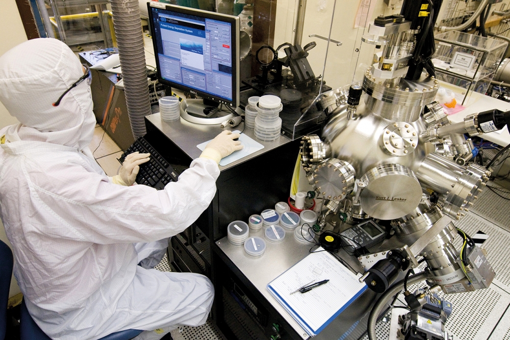
Our team at the US Air Force Research Laboratory is taking on this challenge. Our efforts allow us to work with a highly conductive layer and a substrate that is transparent, thanks to a 4.6 eV bandgap (see Figure 1 for how β-Ga2O3 and SrSnO3 are expanding the capability of the portfolio of high conductivity TCOs).
In our work, we have grown homoepitaxial silicon-doped Ga2O3 layers by pulsed laser deposition on semi-insulating, iron-doped Ga2O3 (010) single-crystal substrates from Novel Crystal Technology. Our film growth involved directing a KrF excimer laser, operating at a 10 Hz repetition rate and providing an energy density of 3 J cm-2, at a Ga2O3 - 1 wt. percent SiO2 ablation target. We deposited our films under argon at a pressure of 13 Pa, using a substrate temperature of 590 °C.

Figure 1. Film conductivity as a function of wavelength for TCOs. Until
the recent discovery of wide bandgap β-Ga2O3 and SrSnO3 there had been
an abrupt boundary at around 330 nm (3.8 eV). The purple shaded region
associated with the right Y axis corresponds to a portion of an optimal
window transparency extending into the UV range. Adapted from Zhang et
al. Nature Materials 15 204 (2016).
Armed with attributes
To elucidate film quality, we undertook structural and chemical analyses of our material. X-ray diffraction rocking curves revealed a sharp film peak overlapping the substrate peak, indicating high-quality epitaxy. For silicon-doped β-Ga2O3 films with thicknesses from 40 nm to 512 nm, the average [020] full-width at half-maximum is 46.8 arcsec, compared with 32.4 arcsec for the β-Ga2O3 substrate.
Scrutinising β-Ga2O3 films with atomic force microscopy revealed a smooth surface. Its root-mean-square roughness is about 0.4 nm, only slightly rougher than that of the bare substrate, which has a value of around 0.1 nm.
The chemical content throughout our β-Ga2O3 layer is uniform, according to depth profiles obtained by secondary-ion mass spectrometry (SIMS) of silicon and iron in a 512 nm-thick representative film. Measuring the silicon level allowed us to determine the extent of chemical incorporation in this layer. Meanwhile plotting the iron concentration enabled us to find out if any of the compensating iron in the substrate, added to make it insulating, out-diffused into the film. As the concentration of iron is around 1017 cm-3, it has no impact on film conductivity, and is far below the silicon-dopant level of 3 x 1020 cm-3.
We turned to Hall-effect measurements to evaluate the transport properties of our oxide. These measurements indicate a room-temperature conductivity of 2323 S cm-1, approximately a quarter of the value for ITO of 1 x 10⁴ S cm-1. Resistivity is 4.3 x 10⁻⁴ Ω-cm, carrier concentration 2.24 x 1020 cm-3 and mobility of 64.5 cm2 V-1 s-1 (see Figure 1). To form ohmic contacts we deposited a Ti/Al/Ni/Au stack on the sample corners, before annealing this structure for 1 minute at 470 °C under a flow of nitrogen gas.
Comparing the charge carrier concentration obtained by Hall measurements to the silicon concentration, determined by SIMS, enabled us to calculate values for the electrical activation efficiency of 77 percent for a 40 nm-thick film, and 56 percent for a 512 nm-thick film. For those of you interested in a detailed analysis of the relationship between doping and Hall-effect results in silicon-doped β-Ga2O3, take a look at the box “Delving in to doping”.
Confirmation of our film’s structure and its quality has been provided by high-resolution scanning tunnelling electron microscopy. Images obtained with this form of microscopy show bright contrast at the interface between the film and substrate, likely originating from point defects. While this film is in the form of the β-phase, there is a very thin surface layer of γ-Ga2O3 [110], less than 1 nm-thick. Note that a γ-Ga2O3 surface layer has also been observed in β-Ga2O3 films grown by MBE, suggesting that the γ-Ga2O3 surface layer occurs due to an intrinsic growth mechanism during homoepitaxial β-Ga2O3 [010] deposition.

Figure 2. X-ray diffraction rocking curves (a), atomic force microscopy
surface scan (b), secondary-ion mass spectrometry depth profile (c) and
cross-sectional transmission electron microscopy images (d) of
homoepitaxial silicon-doped β-Ga2O3 films grown by pulsed laser
deposition on iron-doped β-Ga2O3 substrates. Adapted from Jeon et al.
APL Materials 9 101105 (2021).
To assess the transparency of this TCO over a wide spectral range, we have undertaken transmittance and reflectance measurements from 190 nm to 3200 nm (6.52 eV to 0.387 eV). These studies, considering a 512 nm-thick silicon-doped β-Ga2O3 film grown on a double-side polished β-Ga2O3 substrate, reveal transmittance and reflectance, while allowing us to calculate absorbance (see Figure 3). According to these measurements, optical transmittance is about 70 percent from 3.7 eV (335 nm) to 0.56 eV (2214 nm), and falls in the deep UV, reducing to 20 percent at 4.42 eV (280 nm). In this region, the optical transmittance of the highly conductive silicon-doped β-Ga2O3 is much smaller than that of the undoped β-Ga2O3 – for example, it is roughly half at 280 nm. We have also found that the bandgap of this highly conductive β-Ga2O3, having a value of around 4.596 eV, is below that of undoped β-Ga2O3, which is typically 4.9 eV. We consider this to be the result of competition between a lower conduction-band edge and a higher Fermi level, both due to heavy doping.
Our primary motivation for developing epitaxial β-Ga2O3 is that this material can serve in power devices, such as lateral and vertical FETs and Schottky barrier diodes. All these devices promise to capitalise on the theoretical critical field strength of β-Ga2O3 – it can withstand fields as high as 8 MV cm-1. As it is possible to n-type dope β-Ga2O3 over a large carrier concentration range, this will open the door to a number of intriguing possibilities for advanced device operation.
There are several reports of the Hall-effect mobility versus carrier concentration for β-Ga2O3 films formed with a variety of deposition techniques and containing different dopants (see Figure 4). This body of work, published since 2012, includes films formed by MBE, MOCVD, HVPE, low-pressure CVD, mist CVD and pulsed laser deposition. According to literature, silicon, tin and germanium are the principal dopants investigated so far, and the preferred β-Ga2O3 substrate orientation is (010). There are fewer reports using (001) and (100).
We have identified three ranges of carrier concentration, corresponding to notional functional regimes. For high-power vertical devices blocking 1 kV or more, doping should be below 2 x 1017 cm-3; for lateral power switching, where voltages are below 1 kV, doping is varied from 2 x 1017 cm-3 to 1 x 1019 cm-3; and for optimal device ohmic contacts, doping needs to be degenerate, with a value in excess of 4 x 1019 cm-3. As stated already, our film formed by pulsed laser deposition has a conductivity of 2323 S cm-1 (designated by red stars in Figure 4), and could be used as an improved transistor ohmic regrowth contact layer. In this guise, it has been implemented with moderate success.
In addition to our efforts, other researchers are making improvements to the conductivity of β-Ga2O3 epitaxial film conductivity, using methods that are more scalable and commercially viable. Those at The Ohio State University have used MBE to demonstrate delta silicon-doped layers (structures with alternating highly doped and unintentional doped layers) with a mobility of 83 cm2 V-1 s-1 and sheet resistance of 320 Ohm/sq, and integrated this structure in a FET. Also generating impressive results is the team at the University of Utah, recently reporting a conductivity of 1635 S cm-1 for β-Ga2O3 grown by MOCVD (see Figures 1 and 4). Their technology, specifically developed for realising an improved ohmic contact, enabled them to produce a fully MOCVD-based MESFET with channel layer, using a 600 °C regrowth process yielding a 73 Ohm/sq sheet resistance. At the U.S. Air Force Research Laboratory, we continue to refine our pulsed laser deposition process to realise higher conductivities. We hope it will not be long before our higher conductivity data, along with improved results from groups using MOCVD and MBE, will be shared.
Striking stannates
Within the ultra-wide bandgap TCO landscape, β-Ga2O3 is not alone; new reports of TCO stannates are equally intriguing. As one might expect, results vary, depending on the composition of the stannate. For BaSnO3 doped with lanthanum, conductivity is excellent, at around 104 S cm-1, but the bandgap is just 3 eV. More promising is lanthanum-doped SrSnO3, exhibiting a conductivity of 2930 S cm-1 (plotted in Figure 1) and an estimated bandgap of 4.6 eV, according to results at Hokkaido University using MgO substrates, pulsed laser deposition and a growth temperature of 790 °C.
It’s worth noting that in stark contrast to the single-crystal epilayer formed during homoepitaxial β-Ga2O3 growth, these heteroepitaxial SrSnO3 films have a distinct grain structure. Although this compromises crystal quality, it is beneficial on one front: the lateral grain growth from a 790 °C post-deposition vacuum anneal increases the activation efficiency of the lanthanum ions, and ultimately boosts conductivity.
Researchers at the University of Minnesota have also been exploring the potential of stannates. They have reported a conductivity of 2157 S cm-1 for neodymium-doped SrSnO3 grown on a lattice-mismatched GdScO3 substrate with an undoped buffer layer (see Figure 1). While this team did not measure the bandgap of their oxide, they indicated that it is likely to lie between 4.1 eV to 4.6 eV. The mid-point of this range has been adopted in Figure 1.
By turning to non-native substrates and polycrystalline morphology, those working in this field now have many exciting avenues for future device development. ITO and ZnO-based films have a tremendous advantage in this regard, as they are generally substrate agnostic, with polycrystalline or amorphous films resulting. As previously stated, stannates also offer some versatility, as they can be grown on MgO or other substrates. However, it is worth considering that many device demonstrations already accomplished with the β-Ga2O3 system and its native substrate have drawn on the opportunity to add charge carriers, either by doping during epitaxial growth or by ion implantation – both are commercially viable processes. With the stannate system, which is not as advanced as β-Ga2O3, device demonstrations are yet to be reported. However, neodymium-doped SrSnO3 has shown a very promising mid-level doping of 3.7x1018 cm-3, suggesting that it might be suitable to modulation.
It is routine to form high-quality β-Ga2O3 films on native substrates. Fortunately, these substrates can be produced from the melt. That has helped to support rapid device development, and enabled the demonstration of substrates up to 100 mm in diameter. Today, the primary method for making semi-insulating β-Ga2O3 substrates is edge-defined film-fed growth, a process used by Novel Crystal Technology and widely adopted for producing sapphire. Meanwhile, growth of β-Ga2O3 by the Czochralski method, which has long been utilized for making silicon wafers, is under development by Northrop Grumman Synoptics.

Figure 3. Transmittance, reflectance, and absorbance measurements made on
a 512 nm-thick silicon-doped β-Ga2O3 [010] (a). The purple shaded
region corresponds to an optimal transparent window. Measured bandgap
energy of 4.595 eV from a silicon-doped β-Ga2O3 [010] film (b). Adapted
from Jeon et al. APL Materials 9 101105 (2021). The bandgap has been
calculated from a linear plot of α2 versus energy E. The absorption
coefficient α is calculated from a formula that holds for small α as
well as large α. (Note that the usual Tauc plot of (αE)2 versus E is
correct only for amorphous materials.)
Possible pathways
What should be the next step for wide bandgap TCOs? Although not capitalizing on their material transparency, one immediate integration path is their expanded use as regrowth layers for β-Ga2O3 FETs. Efforts in this direction would be beneficial, given that despite significant progress in β-Ga2O3 power devices over the last ten years, low-resistivity ohmic contacts are immature and not widely integrated. Note that other techniques, such as spin-on-glass and ion implantation, have also been developed to target lower contact resistance.
A second implementation path entails solar-blind detectors, a class of device that is sensitive to light at wavelengths shorter than 280 nm. When deep-UV photodetectors operate at high temperatures, they have the potential to serve in space communication, UV astronomy, and pollution analysis. Conventional UV photodetectors are impaired by their high dark current leakage, attributed to the narrow bandgap of the silicon-based structures. Switching to wide bandgap materials with high conductivity expands the range of radiation detection, to cover the optical spectrum into the ultraviolet domain, while improving high-temperature performance. Options include SiC, GaN, ZnO, and β-Ga2O3. However, SiC, GaN, and ZnO have bandgaps narrower than 4.42 eV, so alloying with another element is needed to increase the bandgap to this critical value and limit absorption of light to wavelengths below 280 nm. Alloying is far from ideal, though, as it leads to large defect densities associated with lattice mismatch.
A more promising candidate is β-Ga2O3, which is intrinsically suitable for deeper UV photodetectors – that is, no alloying is required. The pairing of highly conductive β-Ga2O3 with a native substrate leads to fewer defects and potentially benefits from homogenous thermal expansion. Note that as β-Ga2O3 has a low thermal conductivity, additional studies are required to assess potential thermal limitations.
Another weakness of traditional silicon-based photodetectors is the need for significant cooling to improve the external quantum efficiency. While photodetectors based on β-Ga2O3 are in their infancy, initial demonstrations provide a promising performance and uncooled operation, indicating that these devices are a potential alternative to solar-blind detectors made with other materials.
Finally, there is the possibility of improving the capability of β-Ga2O3 by alloying it with another material and realising an even higher bandgap. Using MOCVD, β-Ga2O3 alloyed with 33 percent aluminium yields a mid-1018 cm-3 carrier concentration. Building on this is the fabrication of an aluminium-alloyed Ga2O3/Ga2O3 stack that creates a highly conductive thin channel (2DEG) at its interface. The mobility of electrons in the channel is high as impurity scattering is avoided. It is possible that superlattice-based aluminium-alloyed Ga2O3/Ga2O3 on a native substrate will provide sufficient conductivity as a deeper UV TCO material.
We see the realization of high conductivity in β-Ga2O3 and SrSnO3 as a watershed moment for envisioning TCO applications that extend ‘deep’ into the UV. With our pulsed laser deposition process we have produced β-Ga2O3 with a conductivity of 2323 S cm-1, but the electrical activation efficiency and transmission in the UV are far from ideal. It is paramount to undertake further studies and realise even higher conductivities. We predict that this is possible by increasing the electrical activation efficiency to around 90 percent.
That’s by no means the only challenge to address to make these materials relevant and useful for TCO-centric applications. There’s much to do, as efforts must be directed at substrate development, mitigation of low conductivity, compatibility with other layers and processing requirements, ensuring short- and long-term stability under environmental conditions, and introducing complimentary p-type materials. Motivating all this work will be fulfilling the promise of β-Ga2O3, which has great potential as a TCO and beyond. Figure 4. Hall effect mobility versus carrier concentration for n-type homoepitaxial β-Ga2O3 films in the recent literature. Data points in the legend are identified by deposition technique, dopant (if used), substrate orientation and year of publication. Adapted from Jeon et al. APL Materials 9 101105 (2021).
DELVING IN TO DOPING
Highly-doped semiconductors often experience self-compensation, a process in which a dopant produces donors and acceptors, instead of just one or the other. In the case of silicon-doped β-Ga2O3 we expect silicon atoms to occupy gallium sites and produce SiGa donors (charge ZD = +1) that result in n-type conductivity, which is observed. However, to minimise the energy of the crystal, acceptors are incorporated by generating gallium vacancies VGa. These defects are triple acceptors (charge ZA = -3) that, as well as reducing the free electron concentration, greatly increase electron scattering, varying as ZA2. According to density functional theory, silicon-related acceptor complexes SiGa-VGa (ZA = -2) and 2SiGa-VGa (ZA = -1) can also form, providing another drag on concentration and mobility.
We have used temperature-dependent Hall-effect measurements to determine donor ND and acceptor NA concentrations as a function of measured mobility and free-electron concentration for each possible value of acceptor charge ZA = -1, -2, or -3. More recently we have modelled 40 nm-thick and 512 nm-thick silicon-doped β-Ga2O3 films that have silicon concentrations of 3 x 1020 cm-3 and 4 x 1020 cm-3, respectively, according to SIMS. For the special case of the three possible acceptor charges being equally likely, Hall-effect analysis predicts silicon concentrations of 3.0 x 1020 cm-3 and 3.7 x 1020 cm-3, respectively. As these numbers are so close to the SIMS results, the case of three possible acceptor charges is certainly a valid possibility. However, another possibility is that the charge ZA = -2 is dominant, in which case the Hall-effect prediction would be 2.6 x 1020 cm-3 and 3.2 x 1020 cm-3, respectively.
While more data are required to reach a rigorous conclusion, the Hall-effect model appears to be valid and well worth exploring in greater detail. Indeed, if gallium vacancies are responsible for most acceptors, it is well worth exploring approaches that reduce their concentration. Applying this strategy to gallium-doped ZnO is known to deliver success, with zinc vacancies greatly reduced when annealing the sample face down on a zinc foil under a forming gas ambient.
Further reading
† Jeon et al. “Homoepitaxial β-Ga2O3 transparent conducting oxide with conductivity β = 2323 S cm-1,” APL Materials 9 101105 (2021)
† Wei et al. “High electrical conducting deep-ultraviolet transparent oxide semiconductor La-doped SrSnO3 exceeding ~3000 S cm-1,” Appl. Phys. Lett. 116 022103 (2020)
† Truttmann et al. “Combined experimental-theoretical study of electron mobility-limiting mechanisms in SrSnO3,” Comm. Physics 4 241 (2021)
† Bhattacharyya et al. “130 mA mm-1 β-Ga2O3 metal semiconductor field effect transistor with low temperaturemetalorganic vapor phase epitaxy-regrown ohmic contacts,” Appl. Phys. Exp. 14 076502 (2021)
† Prakash et al. “Wide bandgap BaSnO3 films with room temperature conductivity exceeding 104 S cm-1,” Nature Communications 8 15167 (2017)
† Kang et al. “Fundamental limits on the electron mobility of β-Ga2O3,” J. Phys. Condens. Matter 29 (2017)
† Look et al. “Classical and quantum conductivity in β-Ga2O3,” Sci. Rep. 9, 16 (2019)
† Look et al. “Stable highly conductive ZnO via reduction of Zn vacancies,” Appl. Phys. Lett. 101 102101 (2012).
† Tak et al. “High-temperature photocurrent mechanism of β-Ga2O3 based metal-semiconductor-metal solar-blind photodetectors,” J. Appl. Phys. 125 (2019)
† Krishnamoorthy et al. “Delta-doped β-gallium oxide field-effect transistor,” Appl. Phys. Exp. 10 051102 (2017)
† Bhuiyan et al. “MOCVD epitaxy of β-(AlxGa1−x)2O3 thin films on (010) Ga2O3 substrates and N-type doping,” Appl. Phys. Lett. 115 1 (2019)


