
MicroLEDs propel UVC output
An array of UVC microLEDs that is the size of a standard chip delivers an output power of over 80 mW
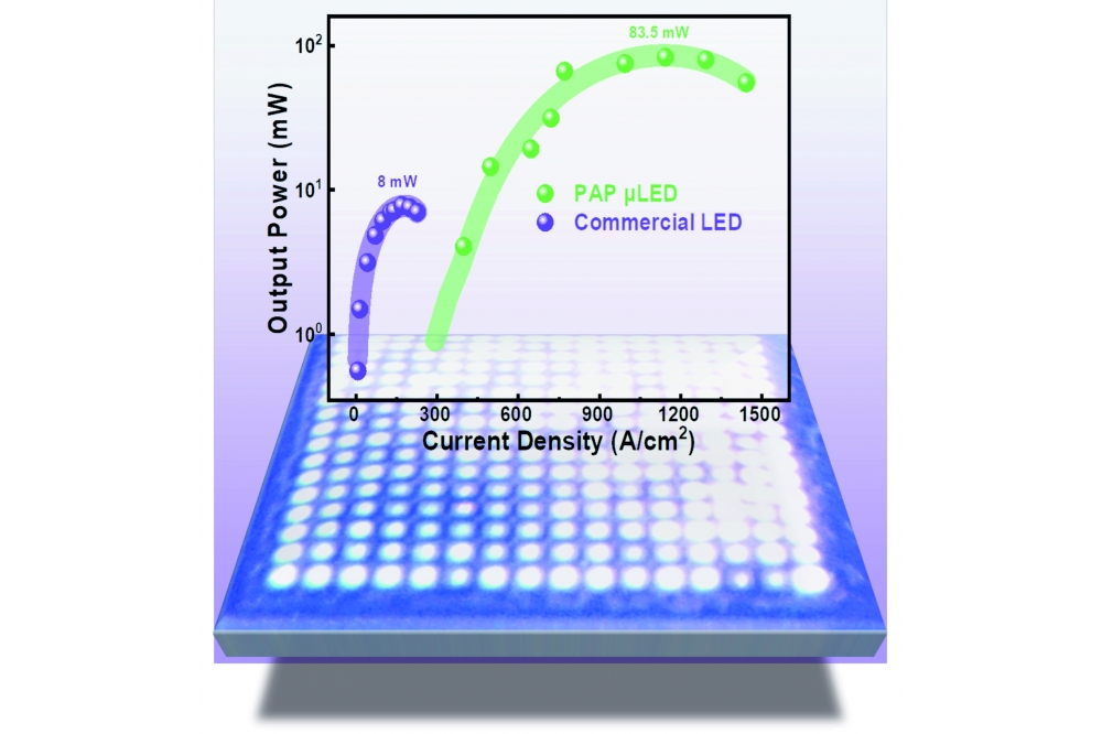
LEDs operating in the UVC – that’s the spectral domain that spans 200 nm to 280 nm – are renowned for a feeble output. But this reputation should soon be shattered, thanks to a collaboration in China led by Peking University that has broken new ground for the output power from a standard-sized chip. The team’s best device, containing 16 by 16 microLEDs and emitting at 280 nm, produces more than 80 mW output when driven at 230 mA.
According to team spokesman Xinqiang Wang from Peking University, the very strong emission produced by these LEDs stems from realising a high wall-plug efficiency at a high injection current.
“Conventional state-of-the art planar deep-UV LEDs at 265–280 nanometres typically show their highest value of wall-plug-efficiency at a very small current density, typically lower than 50 A cm−2,” remarked Wang. Due to this, conventional devices are only capable of a low light output power.
“In our work, both the light output power and the wall-plug efficiency of our parallel-array planar microLEDs reached their maximum values at current densities larger than 700 A cm−2, making them quite preferable for practical applications,” added Wang.
As well as being suitable for many of the applications often discussed for UVC LEDs, such as a disinfection and curing, they could be used for free-space communication, thanks to their high modulation speed.
Emitting at 280 nm, the team’s UVC LEDs are within the solar blind region, enabling communication that avoids interference from ambient conditions. Another merit of using such short wavelengths is that it allows non-line-of-sight communication, thanks to abundant atmospheric scattering by molecules and aerosols.
The parallel-array planar LEDs developed by Wang and co-workers have several features that help to increase light output power and wall-plug efficiency. Microcontacts are introduced on top of the p-GaN to trim absorption from the p-type ohmic contact, and the cylinder-shaped mesa is coated with an aluminium mirror to ensure isotropic light extraction (see Figure). In addition, the device is designed to ensure a homogeneous current distribution; the size of the emission region is reduced to enable a higher current density; and tensile stress is reduced with a smaller mesa size, decreasing the proportion of transverse-magnetic polarised light that hampers light extraction.
A range of devices have been produced by the team: a 16 by 16 array with 25 µm-diameter emitters; an 8 by 8 array with 50 µm-diameter emitters; a 4 by 4 array with 100 µm-diameter emitters; and a 2 by 2 array with 200 µm-diameter emitters; and a conventional control, fabricated from the same wafer. All variants have a total emission area of 0.125 mm2, equal to that for a conventional device.
The control produced a peak output of 8 mW at 170 A cm−2. This output power exceeded that for devices with emitters with diameters of 50 µm or more, although they peaked at high current densities. In stark contrast, the device with a 16 by 16 array of 25 µm-diameter emitters delivered an output power of 83.5 mW at a current density of 1150 A cm−2, while the wall-plug efficiency peaked at 4.7 percent at 775 A cm−2. Superior performance is attributed to a suppression of light absorption and a homogeneous injection current.
For solar blind communication, the more powerful device has the most promise, as its high light output power at a high current density, allied to its small size, has the greatest potential for realising a high modulation bandwidth over a long distance. Measurements on this device using orthogonal frequency-division multiplexing revealed a data rate of just over 1 Gbit/s at a bit-error rate of 1.3 x 10⁻².
One of the next goals for the team is to fabricate parallel-array planar deep-UV micro-LEDs with even smaller pixel size, for example, 1 or 2 micrometers. Another aim, according to Wang, is to promote the commercialisation of this architecture.
Reference
D. Li et al. Adv. Mater. 210975 (2022)


