
UVC laser delivers continuous-wave emission
Combining a pair of n-type electrodes with increased optical confinement enables the first continuous-wave emission in the UVC
A team of researchers from Japan is claiming to have produced the first laser diode that delivers continuous-wave emission in the UVC, which is the spectral range spanning 280 nm to 200 nm.
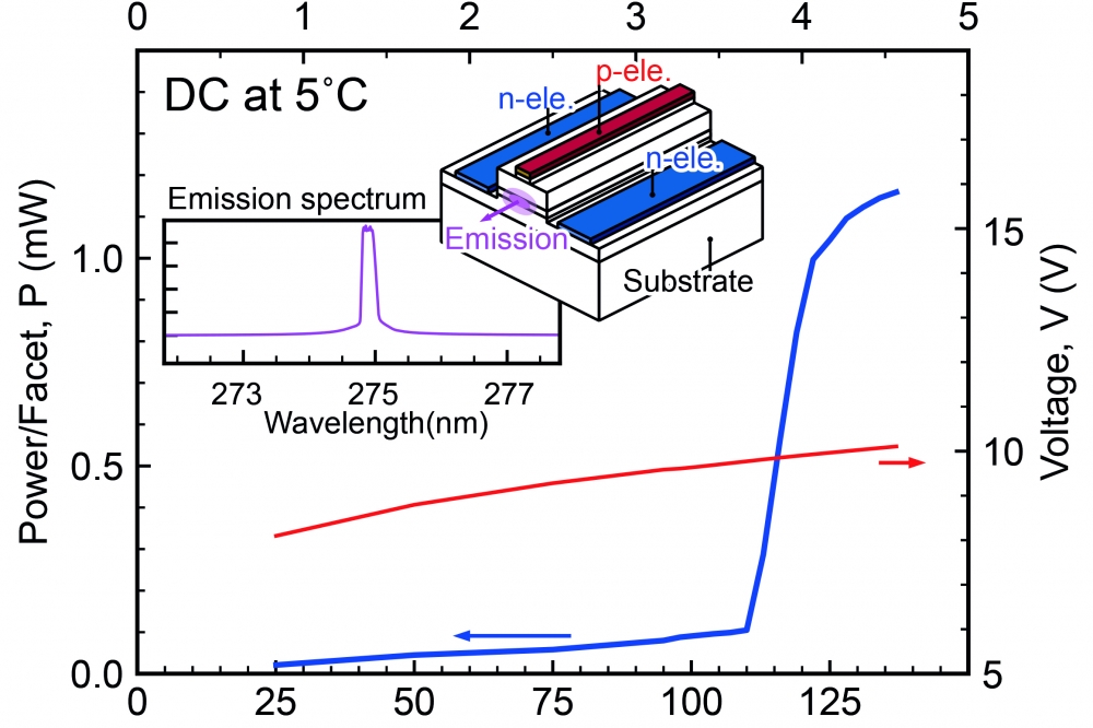
Operated at 5 °C, the device produced by the partnership between Asahi Kasei Corporation and Nagoya University emits an output power of just over 1 mW at 275 nm.
“We believe the accomplishment reported here is a leap towards a practical UVC laser diode,” remarked team spokesman Ziyi Zhang, who is affiliated to both Asahi Kasei and Nagoya University. According to Zhang, a UVC laser could be deployed for various tasks, including biological and chemical sensing, particle detection, rapid sterilisation, solar blind communication and materials processing.
The team’s triumph came from combining recent breakthroughs in UV laser design with the introduction of an architecture with a higher degree of optical confinement and the addition of a pair of n-type electrodes. The UVC resulting continuous-wave laser, which is grown on free-standing AlN, features: an active region with a high internal quantum efficiency; polarization-induced doping; a cladding layer that ensures greater optical confinement; and a pair of n-type electrodes, added to the top surface.
Note that while n-type electrodes are normally placed on the back surface of a laser diode to ensure a low-device resistance, this is not the first time that they have been added to the top of this class of device. Such a configuration has been employed before for lasers grown on sapphire.
Zhang and co-workers made their breakthrough by evaluating the performance of a portfolio of devices produced by MOCVD on the aluminium face of single-crystal AlN substrates.
The team produced a control by depositing an epitaxial stack that contained a 350 nm n-type silicon-doped Al0.7Ga0.3N cladding layer, a 100 nm-thick Al0.63Ga0.27N waveguide containing a pair of 4.5 nm-thick quantum wells, a 320 nm-thick p-type distributed polarization-doped cladding, and a p-type contact layer. Dry etching and cleaving created a device with a 5 mm-wide mesa stripe and a 600 mm-long cavity. To increase facet reflectivity to 90 percent, the team deposited 5 pairs of HfO2/SiO2.
A variant with a Al0.75Ga0.25N cladding layer allowed Zhang and colleagues to consider the implications of differences in the optical confinement in the quantum well. Increasing the aluminium content lowered the refractive index, cut the leakage of optical modes and reduced the threshold current under pulsed-mode operation. However, all of this came at the expense of an increase in series resistance.
Building on this insight, the team went on to produce a pair of devices – they only differed in having either one or two n-type electrodes beside the mesa stripe. Both designs had a higher quantum efficiency than their predecessors, thanks to a reduction in point defects in the quantum wells.
Electrical-optical pulsed measurements on these devices, packaged in TO-cans, revealed a threshold current density of just 2.8 kA cm-2 for both devices, attributed to the increase in internal quantum efficiency. Switching from a single n-type electrode to a pair of them trimmed the resistance from 20 W to 12 W and enabled the first CW emission. Lasing began at 110 mA, corresponding to a threshold current density of 3.7 kA cm-2.
According to the team, efforts should now be directed at realising a lower threshold current density for CW lasing. This could come from a higher internal quantum efficiency and an increase in the injection efficiency, which is probably still below 10 percent – in comparison, that figure for the InGaN-based laser diode is typically 60 percent or more.
Zhang revealed that he and his co-workers will continue to improve their device, with the goal of producing a UVC laser with a performance suitable for user testing.
“Given the history of laser diode development at any wavelength range, achieving continuous-wave oscillation at room temperature is the next milestone for device performance.”
Reference
Z. Zhang et al. Appl. Phys. Express 15 041007 (2022)


