
Faster feedback refines VCSEL production
A novel wafer-scale ‘quick-fab’ process aids VCSEL manufacture by providing rapid device feedback.
BY SAMUEL SHUTTS FROM CARDIFF UNIVERSITY
DEMAND FOR THE VCSEL shows no sign of slowing. Sales took off with deployment in wireless data communication, reached a new high when its use extended to face-and-gesture recognition systems in smartphones, and will jump again through the roll out of lidar systems in autonomous vehicles. Due to this continuous ramp in demand, VCSEL manufacturers are under increasing pressure to ship more devices.
To cater for this growing demand, makers of GaAs-based VCSELs have moved to ever larger wafer sizes – a move that as well as increasing volume, addresses the call to drive down the cost per device. As far back as 1994, the world’s leading supplier of epiwafers, IQE, signed its first commercial contract for 75 mm wafers, and demonstrated its capability to produce these heterostructures on 100 mm wafers – although it wasn’t until 2013 that mass-production kicked-off on this large size. Since then progress has accelerated. 150 mm wafers that are capable of providing 200,000 devices were introduced in 2014, and this May IQE introduced the world’s first commercially available 200 mm VCSEL wafer, enabling further expansion of the sensing market.

Figure 1. IQE’s VCSEL production timeline. Courtesy of IQE.
The need for quick-fab
Alongside increases in the production throughput of the VCSEL, realised partly through the migration to larger wafers, there has been a tightening of tolerances to meet the more stringent demands of emerging applications. Due to this state-of-affairs, there is an ever-increasing need for device-level characterisation that delivers a rapid assessment of wafer uniformity and exposes any drift occurring during a manufacture cycle. Such a service complements the production-line characterisation toolkit by providing active device data.
Our team, a collaboration between Cardiff University and IQE, has striven to develop such a service through a project entitled ATLAS, Advanced manufacturing Techniques for semiconductor LASers. This effort has focused on drastically reducing the time taken to fabricate a conventional VCSEL structure by utilising a simplified strip-backed process, which can provide fast feedback to production teams. The aim has been to complete fabrication within 24 hours.
The proposed ‘quick-fab’ VCSELs are not intended for packaging as individual chips, employed in end-user technology. However, they do need to be compatible with automatic wafer-level probing, which enables the mapping of various characteristics, including the VCSEL’s emission spectrum and its optical output power as a function of current and voltage. From these measurements it is possible to extract key characteristics for this class of laser, such as its threshold current (the minimum current required to realise laser action), its power-conversion efficiency and its peak wavelength.

Figure 2. Cross-section of a typical VCSEL design, with SEM image showing an etched mesa structure.
An additional benefit provided by a quick-fab service is that it allows VCSEL manufacturers and their customers to develop new products more efficiently. VCSELs are complex structures, comprising up to 200 or more layers, each with a carefully controlled composition and a thickness ranging from 1 µm down to as little as 4 nm. While simulation software supports the design of a new VCSEL, to satisfy an intended application this often has to be accompanied by a design-of-experiment. To optimise device performance, engineers tend to use several reiterations of design, epi-wafer growth and VCSEL fabrication. Our VCSEL technology quick-fab supports such endeavours, providing process monitoring and aiding R&D and product development.
Note that the benefits of VCSEL quick-fab are not limited to producing devices for large consumer markets. This form of fast-feedback also has a role to play in supporting the emergence of specialist atomic sensor technologies, such as miniature atomic clocks, magnetometers and quantum gyroscopes. All these technologies call for stringent VCSEL specifications. For example, caesium-based atomic sensors require stable single-mode sources targeting atomic transitions at 894.6 nm and 852.347 nm. Hitting these transitions requires some current and temperature tuning, but ideally this is minimal, to ensure high efficiency and lessen the impact on the environment of the accompanying caesium vapour cell.
There is yet another benefit of VCSEL quick-fab, related to a predominant design challenge. With this class of laser it is crucial to have a healthy overlap between the optical gain spectrum and the resonant cavity mode. That’s because the VCSEL cannot operate over a wide range; rather, it is constrained to emit at a particular wavelength by virtue of its optical design. To ensure efficient operation, the peak of the gain has to align with the cavity mode. This situation is analogous to shining a torch through a keyhole, where alignment is essential to enable efficient transfer of light. Sub-optimal alignment can be compensated by increasing the brightness of the torch, but this comes at the expense of consuming more energy.
Complicating matters, both the peak of the gain spectrum and the location of the cavity mode shift with temperature, and they do so at different rates. A prudent designer accounts for this, targeting the gain peak and cavity resonance to coincide at the designed temperature and operating current. Quick-fab VCSELs can speedily determine if this is actually the case.
The quick-fab concept
One of the attractive features of the VCSEL is the relative ease of large-scale manufacture. As all the light is emitted vertically from the surface, engineers undertake on-wafer testing, rather than cleaving material into individual chips, as is the case with edge-emitting lasers. However, fabricating VCSELs is not that simple. It is certainly not trivial to confine light and current in localised regions – and these are pre-requisites for efficient operation.
The widely adopted approach for ensuring localisation of electro-optical processes is to etch a mesa structure into the epiwafer to a depth that exposes an oxidation layer buried within the VCSEL structure (see Figure 2). This layer, formed from aluminium-rich AlGaAs, is partially oxidised to form an aperture or window in the centre of the mesa that defines the path for current flow. One of the merits of this approach is that it also guides light within the same region, thanks to the resulting refractive index profile.
Unfortunately, in a conventional VCSEL, it is not possible to connect an electrical wire or probe directly to the mesa, because it is too small. Due to this, the mesa is first ‘planarized’ with an electrically insulating material, before a feed metal interconnect and a relatively large metal contact pad are deposited. These steps eat up time. To enable VCSEL quick fab, an approach must be taken that mitigates planarization and subsequent metallisation.
Our solution involves defining a mesa structure by etching the semiconductor epiwafer, an approach that’s similar to that employed for making a conventional VCSEL – but in our case we leave portions unetched, which are subsequently used to support the electrical interconnect and contact pad. We ensure that current only flows through the VCSEL aperture by etching vias to expose the aluminium-rich layer, which is subsequently oxidised in all regions, except for the area prescribed by the VCSEL aperture. Following this, we added a topside metal p-contact and back-side n-contact, before annealing to produce low-resistance ohmic contacts (see Figure 3 for an SEM image of our device and accompanying schematic showing a cross-section).

Figure 3. (left) Isometric SEM micrograph of a fabricated VCSEL
quick-fab device taken using a Hitachi SU8320 housed in the Cardiff’s
ICS cleanroom. False colour rendering has been applied to illustrate the
electrical contact pad. (right) An accompanying schematic of a device
cross-section.
With our approach the number of steps required to produce a VCSEL is slashed from around ten to just four. Thanks to this, VCSEL quick-fab trims fabrication time by 60 percent.
For a given mesa size, the size of the oxide aperture tends to vary across the wafer. Differences in dimensions arise primarily from: compositional non-uniformities in the aluminium-rich layer, occurring during epitaxial growth; and variations in the oxidation conditions across the wafer, namely temperature. The implication is that VCSEL performance varies across a wafer.
VCSEL quick-fab offers insight into this variation. What’s more, by using a range of mesa sizes, the influence of variations in fabrication, such as differences in oxidation, can be disentangled from changes in device performance caused by epi-wafer growth conditions. Obviously, this is only possible when the oxidation extent across the wafer is known. We uncover this by incorporating oxidation test-structures into the quick-fab mask design (an example is shown in Figure 4, following the oxidation step). Taking this approach allows us to accurately determine the extent of oxidation via microscopy. When metal contacts are applied, we can confirm the extent of oxidation by electrical conductance measurements. 
Figure 4. Microscope image showing oxidation calibration mesas after
oxidation, with the central dark spot identifying the aperture
(unoxidised region).
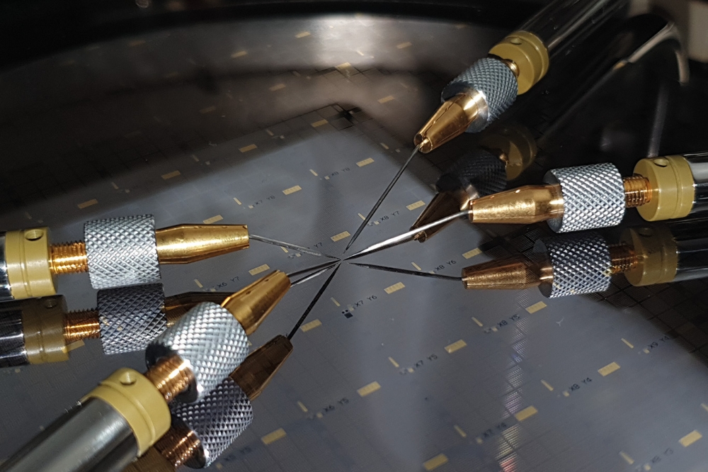
We have applied our versatile VCSEL quick-fab process to a variety of epitaxial structures. One example is a 150 mm wafer that’s been grown by IQE to its 940 nm emission generic design, and been processed within the Institute for Compound Semiconductors cleanroom at Cardiff University. Full processing of one of these wafers yields more than 150,000 quick-fab VCSELs, as well as various test structures, including those for oxidation calibrations and transmission-line measurements (see Figure 5 for an image of this wafer).

Figure 5. Photograph of a fabricated 150 mm VCSEL quick-fab wafer, processed in Cardiff’s ICS cleanroom facility.
With our Quick-fab VCSELs, we can map the power-current characteristics across the wafer. From this, it’s possible to determine the power-conversion efficiency, the thermal rollover and the threshold current. As the oxidation extent is known at multiple points across the wafer, we are able to calculate current density.
An example of the power-current curves for a quick-fab VCSEL with a 16 m µ aperture is shown in Figure 6 (left) for a temperature range of 30 - 70 ˚C. The wafer-scale colour map in Figure 6 (right) shows the variation in threshold current, which is concomitant with the change in oxidation extent we observe across the wafer.

Figure 6. Power-current characteristics of a 16 µm aperture
VCSEL from 30 to 70 ˚C (left) and contour image showing variation in
threshold current across a 150 mm wafer.
Plots of the lasing wavelength of the quick-fab VCSELs and the cavity resonance wavelength show a similar trend across the wafer, albeit with a slight increase in wavelength for the quick-fab VCSELs (see Figure 7).

Figure 7. (Left) Comparing lasing wavelength (squares) with cavity
resonance at different positions across the wafer. (Right) Threshold
current versus temperature for VCSEL devices at the wafer’s centre and
its edge.
This shift to longer wavelengths is caused by Joule-heating, which must be considered in applications that are sensitive to operating wavelength, such as atomic sensors. VCSEL designers need to account for an increase in lasing wavelength of approximately 0.5 - 1 nm mA-1, as well as variation due to ambient temperature of around 0.07 nm per ˚C. Drawing on a reference (see Figure 7, right), we have compared VCSELs with similar aperture diameters formed from the centre and the edge of a wafer, and observed a variance in the threshold current for a given temperature, with the minimum occurring at a different temperature.
This observation offers an insight into the detuning between the gain-peak and the cavity resonance wavelength, and how this changes with temperature – that’s a significant advantage using quick-fab VCSELs, which provide information that cannot be obtained with standard epiwafer characterisation used in a production line.
Armed with quick-fab data, the designer, epiwafer producer, or end-user can determine whether the epi-design is optimised for the operating temperature of the intended application, and be informed of the expected variation in
device performance from different regions of the wafer.
We are continuing to advance the capability and versatility of our VCSEL quick-fab progress. It is currently being used to assess epiwafers for making VCSELs for use in atomic clocks, as well mapping the performance of VCSELs grown by IQE on germanium substrates, which boast improved uniformity compared with GaAs substrates, due to a reduction of strain-induced wafer-bow.
Project ATLAS is supported by the Welsh Government’s SMART Expertise programme and is part financed by the European Regional Development Fund (ERDF). Support also provided by EPSRC Future Compound Semiconductor Manufacturing Hub (EP/P006973/1) and an EPSRC-funded iCASE PhD studentship, co-sponsored by IQE plc. (EP/T517525/1) Fabrication has been carried out in the Institute for Compound Semiconductors and more details can be found on p. 13 of this issue.
Further reading
† J. Baker et al. IEEE Photonics Journal 10.1109
JPHOT.2022.3169032


