
VCSELs: Integrating backside optics
Equipped with micro-optics, VCSELs are even more attractive candidates
for deployment in smart glasses, face recognition systems, automotive in
cabin-sensing and lidar.
BY STEPHAN GRONENBORN FROM TRUMPF PHOTONIC COMPONENTS
THE VCSEL is the ideal source for delivering infrared illumination for 3D sensing. This class of laser produces a narrow and stable spectrum, switches at very high speeds, and operates over a temperature range that spans from -40 °C to 125 °C. And when it is driven with short pulses, it enables the generation of high-resolution 3D distance maps.
Deployment of the VCSEL in consumer electronics goes back several years. Since 2015, it has been a standard component in smartphones. More recently, applications where it is seeing sales have broadened. Now, as well as assisting with time-of-flight measurements for face recognition and depth sensing in smartphones, VCSELs are serving in world-facing systems in phones, tablets and robots, and even delivering high-power levels needed in automotive and industrial heat treatment processes.
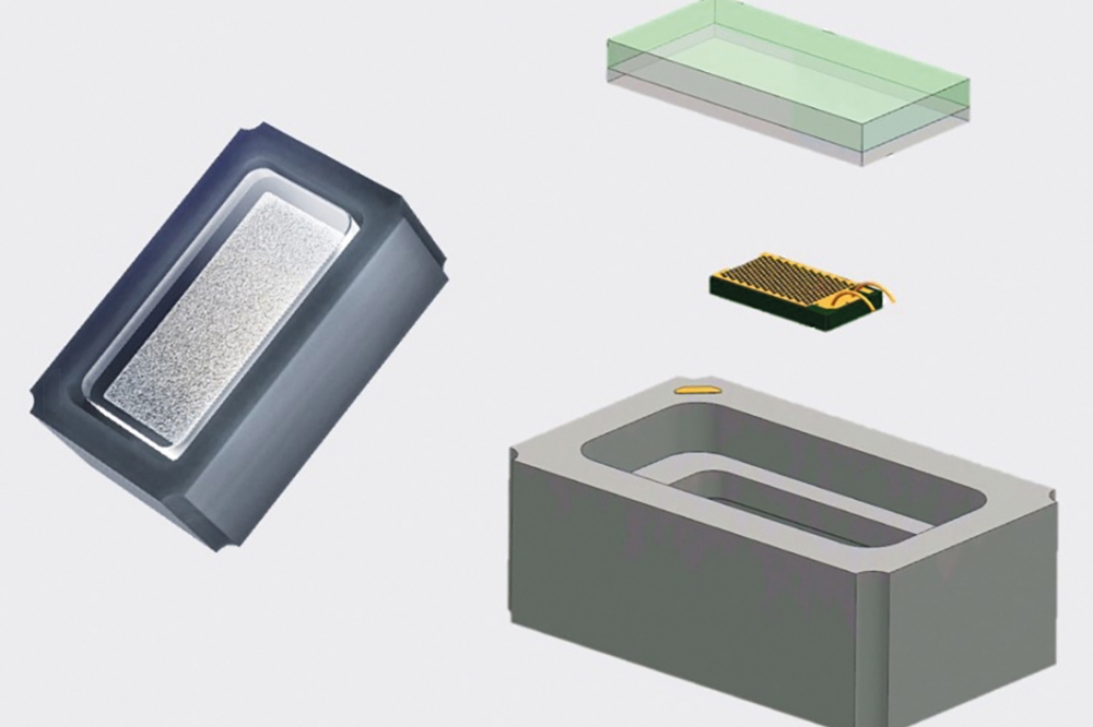
When designers select a bare VCSEL chip, they must package this alongside accompanying optics, connections, driver electronics and safety means. Optics are essential for transforming the beam that emanates from the VCSEL into the desired illumination pattern for the scene. To ensure eye-safety, it is crucial to have correct, properly assembled optics, as well as proper driving of the VCSEL. The downside of this multi-component approach is that by having VCSELs in a separate package, it is impossible to exploit the full potential of the semiconductor production technology, in terms of both footprint and functional integration (this is illustrated in main image).
The VCSEL revolution
At Trumpf Photonic Components we are addressing this shortcoming with a new technology, ViBO, which is short for VCSEL with integrated Backside Optics. Our revolutionary idea is to integrate all optical functions, currently provided by an additional package, directly into the VCSEL chip. The aim is to realise miniaturization while improving performance.
For wavelengths of 940 nm or more, vertical-cavity structures and the transparency of the carrier substrate allow the laser’s emission to exit through the substrate. Adopting this architecture, rather than the conventional one with emission on the epitaxy side, offers a number of benefits that include having hardly any optical losses. Given the attractiveness of this geometry, our efforts towards miniaturization have begun by flipping the direction of the light emission. With light no longer coming out of the surface of the chip, where all the processing and contacting takes place, but through the backside of the substrate, this part of the device is no longer just a mechanical interface but valuable real estate. It is here where we directly etch lenses into the GaAs to provide an optical function and enable extraordinary freedom of design for the customer. Note that the refractive index of the lens is as high as about 3.5, far more than the 1.5 to 2 of plastic and glass, giving much more freedom. What’s more, with our revolutionary design, we eradicate the need for individual alignment of laser die and optics. Instead, the optics becomes an irremovable part of the laser die, and thus a beneficial step for long-term laser safety.
With the processed surface of the chip no longer needed for light emission, this area can be used for electrical, thermal and mechanical functions, enabling optimisation of heat removal and electrical contacts.
One option is to use large contacts on the epitaxy side, enabling direct soldering with flip-chip assembly of the die – this eliminates the need for wire bonds. Merits of this approach are superior thermal management and reduced inductivity of the system. Alternatively, contacts can take the form of slim copper pillars (see Figure 2) enabling SMD mounting to the board or driver IC. Using a large number of such contacts enables individual addressability, and therefore new functionality of the VCSEL chip.
As well as offering the same functionality as the VCSEL in a packaged solution, our ViBO technology has additional benefits that can revolutionize smart-sensing systems. First, the footprint of our ViBO source is five-to-ten times smaller than a traditional VCSEL, and its height is reduced by a similar factor – it is possible to replace a millimetre-thick package with a 150 µm-thick chip. Such miniaturization is highly valued in consumer electronics, including smartphones. Consequently, it is easier to design an entire sensing system with ViBO components, thanks to their diminutive size. Second, our ViBO technology ensures an inherently eye-safe system during the whole product lifetime, because the optics is an irremovable part of the chip. This eradicates safety hazard concerns associated with delaminating or malfunctioning optics. Third, the GaAs optics is more powerful, enabling new designs with superior efficiency. Fourth, new functionalities are possible, as more contacts are on the chip, enabling addressable segments. As these contacts are underneath the surface, the footprint remains small. Fifth, our ViBO technology ensures a longer product lifetime by eliminating additional interfaces. We have eradicated unreliable glue interfaces that threaten to cause problems during the product’s lifetime.

Figure 2. An exemplary ViBO array with the contact side on the left and the lens side on the right.
Yet another strength of our ViBO chips is that they have much in common with high-performance microelectronics. This includes the capability to integrate seamlessly with state-of-the-art silicon packaging technology.
The production of our ViBO chips is based on well-established, mass-manufacturing processes used in the semiconductor industry. We define the lens pattern with grey-tone lithography, using a wafer stepper. Thanks to the high accuracy of this approach, millions of lenses are aligned at the wafer level, rather than in subsequent production steps.
A regular lens pattern that’s designed for uniform illumination of a field-of-view on a scene is shown in Figure 3. Note that no further optics is needed. With this approach illumination fields can vary from the narrow, such as 20 ° by 20 °, to as wide as more than 100 °. It is also possible to tailor the intensity distribution within such a field, allowing more light to be directed towards notoriously dark corners.
Common within the semiconductor industry is bonding with copper pillars. For instance, they are used to create the densely packed connections of a microprocessor. ViBO technology draws on a similar approach (see Figure 3), using lithography to adjust the shape of the pillars. On top of the copper pillar is a solder depot, facilitating the assembly of the chip on ceramic and silicon interposers. Fine pitch patterns support designs with many zones, which can be addressed individually. Many individual VCSELs are grouped into a zone to provide a desired level of power. As the arrangements for the VCSELs and the contacts are independent, and may overlap, this gives more freedom. For example, it allows interlaced and addressing schemes.

Figure 3. Scanning-electron-microscope pictures of the copper-pillar solder bumps (left) and the lens side (right).
Electronic designers also benefit from having both contacts available for addressing – this opportunity enables, for example, the use of a common anode configuration in the driver. Operation in this manner helps to reduce the size of the driver and its power consumption. These merits are particularly welcome in applications with short pulses and high currents, as the driver accounts for a significant part of three key budgets: size, cost and heat.
Turning to a flip-chip assembly that is back-to-back to the driver ensures the shortest connection between the VCSEL and the driver. This configuration is essential for reducing system impedance and enabling the shortest rise and fall times.

Figure 4. A scanning-electron-microscope picture of a demonstrator chip, solder side on the left, lens side on the right.
The perfect match
Using the ViBO platform, chips can be optimized as flood illuminators for indirect time-of-flight cameras. Indirect time-of-flight operation modes are characterized by bursts of pulses, each burst lasting between 100 µs and 1 ms and delivered at a frame rate of 30 Hz to 60 Hz. These requirements for the pulses, along with that for power, may be met with a chip with a surface area of 1250 µm by 940 µm and a height of just 150 µm (see Figure 4). By integrating several hundred lasers on this chip, it can produce the desired power target of 5 W. The solder bumps are separated by 60 µm to ensure a high cross section for efficient heat removal. This chip also features a regular lens array for beam shaping (see the right hand side of Figure 4), that is buried below the level of the outer rim to prevent damage to the lens array from the pick-and-place tool.

Figure 5. Optical power for different operation currents in a typical indirect time-of-flight operation mode with a pulse burst of 400 µs duration at a frequency of 50 Hz. Measurements are made at room temperature (25°C).
Driven at 6 A, this chip delivers the target optical power for this device of 5 W (see Figure 5). At currents beyond this, output power continues to climb.
Our ViBO technology enables flood illumination of the scene that is ‘laser-safe’. One example of this is a beam profile, shaped by integrated optics, that has an angular intensity in the far field with a full-angle half-maximum of 72 ° by 67 °, and an increasing intensity up to 20 ° to the optical axis (see Figure 6). Emission by this chip produces a top-hat irradiance profile on a flat wall on which the camera would be looking to achieve a homogenous camera signal over the image. 
Figure 6. Beam profile: Irradiance on a flat screen (left) and corresponding angular intensity (right).
In comparison, a chip with the same solder interconnect pattern and the same laser arrangement, but without integrated optics, would have a natural divergence of the laser of between 20 ° and 30 ° and a profile that tends to dip in the centre. This noteworthy difference highlights the diffusing effect of beam-shaping optics.
To address this shortcoming in the emission profile, state-of-the-art devices include an external diffusor that’s based on a polymer or glass, often glued into the package. If this diffuser is removed, damaged or immersed in a liquid-like oil, this causes the beam profile to switch from the wide-angle profile of 70 ° by 60 ° to the natural divergence of the laser, just 25 °. An almost seven-fold increase in intensity results, typically creating an unsafe condition for laser illumination.
With ViBO chips, the situation is markedly different. As the optic is integrated, it is impossible to remove it without destroying the laser chip. And due to the high refractive index of GaAs, if the chip is immersed in oil, the intensity only doubles. Thanks to this more modest increase, with ViBO much more power can be designed in the application while retaining laser-safe operation under the failure mode of oil immersion. Note that next-generation devices will encapsulate the ViBO chip with a transparent epoxy to protect it and negate the optical impact of immersion in a liquid.

Figure 7. Pulse shapes of the ViBO chip integrated on a driver and, for comparison, a standard SMD-packaged VCSEL assembled side-by-side to a driver.
A tremendous benefit of flip-chip assembly is that it allows for direct integration with the driver circuit (developed by our project partner iC-Haus), using only a small current loop and without bond wires. With this approach inductance is low, allowing for the very fast rise-and-fall times and steep top-hat pulse shapes that are ideally suited for time-of-flight applications. This strength is illustrated in Figure 7, which highlights the huge difference in rise and fall time for a 10 ns pulse with a 15 A pulse current. One of the four ViBO chips assembled on a driver circuit can be driven with a very rectangular pulse shape, enabling a rise time of only 0.36 ns.
For comparison, we show a state-of-the art VCSEL array in a SMD package, assembled side-by-side to a similar driver in an QFN-package. With this configuration, for the same driving current the rise time (considered to be 10 percent to 90 percent) is 1.65 ns, which is more than 10 percent of the total pulse length. That’s a concern, as for direct time-of-flight methods, a short rise time is strongly connected to the optimum measurement precision.
The future of VCSEL design
According to optical simulations, the same top-hat beam profile can be designed for many different field-of-views of 2D and 3D cameras, ranging from 20 ° to 80 °. Even larger angles up to 150 ° full angle are feasible – we are currently processing demonstrator samples for all these cases. While uniform illumination of the scene is great, there are times when all the action happens in the centre. For these situations, ViBO technology facilitates addressing individual parts of the VCSEL chip, thus illuminating individual zones on the scene and switching off what is not needed (see Figure 8). As well as a hike in efficiency, this feature helps to save scarce battery power and keep the total system cool.

Figure 8. A sketch (top) and simulated beam profiles (bottom) of exemplary laser arrays with several addressable zones to illuminate different regions of interest in the full field of view (60 ° by 45 ° in this example).
Further advantages of using the addressable zones of ViBO are that this can replace the mechanical beam scanners used in automotive lidar, as ViBO has no moving parts. This makes the technology more compact and more reliable. And if larger lidar systems are needed for a longer range, they can be formed by combining several ViBO chips, to increase power and resolution.
We have already tested a first example of a zone-illuminator, using a second variant of the ViBO chips. This investigation did not allow the possibility to address different zones, because we did not include dedicated routing on the interposer and a multi-channel driver.

Figure 9: Beam profile of a ViBO chip illuminating two zones with 15 ° by 45 ° and 20 ° spacing between the zone centres.
The measured beam profile, presented in Figure 9, shows two zones that are clearly separated, and sharp transition regions. Each zone illuminates using a top-hat profile with 15 ° by 45 °, and the zones have a centre-to-centre pitch of 20 °.
Our pioneering work demonstrates that ViBO simplifies the way that VCSELs can be deployed. This new product platform allows 3D sensing systems to be safer, more compact and more cost-efficient. We have no doubt that our ViBO technology will replace assembled VCSEL modules and expand the application scope of VCSELs with new possibilities.
Drawing on planar integration, lithographic methods and fine pitch connectors, ViBO technology is bringing VCSEL production far closer to that used for mainstream semiconductors made of silicon. With this approach, ViBO takes care of the light generation, while silicon serves as the sensor and electronic driver. These developments are destined to fuel the growth of the VCSEL, especially in smartphone and automotive applications.
This work has received funding from the ECSEL Joint Undertaking (JU) under grant agreement No 826600 (project VIZTA) and from the German Federal Ministry of Education and Research under grant agreement 13N14893 (project ALLSTAR). The JU receives support from the European Union’s Horizon 2020 research and innovation programme of France, Sweden, Greece, Spain, United Kingdom, Germany, Luxembourg, Latvia, Hungary. Special thanks go to colleagues from our ALLSTAR project partner iC-Haus for the development and assembly of the driver ICs with the integrated ViBO laser chips.


