
ClassOne Shows New Particle Inspection System at SEMICON West
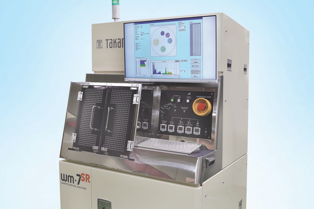
Takano tool for ≤200mm unpatterned wafer inspection offers 61nm particle sensitivity and COP defect detection
ClassOne Equipment will be showing the new high-performance Takano WM-7SR particle inspection system in its exhibit at SEMICON West (July 12-14 in San Francisco).
Designed specifically for ≤200mm unpatterned wafer inspection, this advanced tool now offers an even higher sensitivity option. This enables it to deliver class-leading 61nm particle sensitivity and COP defect detection. The new WM-7SR also features sensitivity mode switching, high dynamic range, and high throughput.
Both ClassOne and Takano personnel will be available at the SEMICON West booth to discuss the process and performance details of this new system.
ClassOne also noted that it has a fully-functioning WM-7SR demonstration system set up in its corporate cleanroom facility in Atlanta. Customer consultations, equipment reviews, and running of samples may also be scheduled there.
In 2022, ClassOne Equipment became the exclusive full-service representative for two new state-of-the-art Takano inspection systems in North America, Europe and Israel. The Takano WM-7SR is designed for inspecting 50mm to 200mm unpatterned wafers and has open-cassette handling. The Takano WM-10 inspects 150mm to 300mm bare wafers with single and dual open-cassette, or single and dual FOUP handler configurations.
ClassOne says the new Takano tools fill a critical need in the semiconductor industry today, replacing long-outdated legacy equipment for inspecting ≤200mm and ≤300mm wafers. It means that users can obtain brand-new particle inspection systems with leading-edge specifications and performance – and at very attractive prices, only marginally higher than refurbished legacy systems.


